home:mbhp:module:din
This is an old revision of the document!
Table of Contents
About
A DIN module is used to connect buttons and encoders to the Midibox. The Name comes from “Digital Input” and means that the module can detect two states: ON or OFF. It then sends this information to be processed by the mbhp core module.It comes with multiple serial registers 74HC165; every register provides 8 digital inputs, which are sampled with the latch enable signal LD and shifted out with the clock signal CLK. The advantage of using such shift registers is, that they can be cascaded to a long chain without the need of more than 5 cables to the core module. The DIN board has been designed on a way which allows to cascade not only the ICs on the board, but also several DIN modules. But note that it depends on the firmware how much inputs are processed by the core module. For instance, the MIDIbox64 allows to connect up to 64 buttons = 8 ICs = 2 * DINX4, the MIDIO128 supports 128 inputs = 16 ICs = 4 DINX4 modules.
Getting Started
Special Instructions
- etc
Details
Pins
DIN & DOUT pin-numbers
The following table shows the relation between pin- and serial-register-numbers on the software side, and physical pins and their labeling on the hardware side. Shiftregisters are always counted from 1 (also on the software-side), and pins are always counted from 0.
Please note that the order of DOUT pins is reversed compared to DIN pins. For a deeper explanation of this issue, refer the information after the table.
Pin table
| Shift Register | SR number | Pin Number (sw) | Pin Hex number (sw) | Pin Name (DIN PCB / SR IC) | Pin Name (DOUT PCB / SR IC) |
|---|---|---|---|---|---|
| first | 1 | 0 | 0x00 | D0 / QA | D7 / H |
| first | 1 | 1 | 0x00 | D1 / QB | D6 / G |
| first | 1 | 2 | 0x00 | D2 / QC | D5 / F |
| first | 1 | 3 | 0x00 | D3 / QD | D4 / E |
| first | 1 | 4 | 0x00 | D4 / QE | D3 / D |
| first | 1 | 5 | 0x00 | D5 / QF | D2 / C |
| first | 1 | 6 | 0x00 | D6 / QG | D1 / B |
| first | 1 | 7 | 0x00 | D7 / QH | D0 / A |
| second | 2 | 8 | 0x0 8 | D0 / QA | D7 / H |
| second | 2 | 9 | 0x0 9 | D1 / QB | D6 / G |
| second | 2 | 10 | 0x0a | D2 / QC | D5 / F |
| second | 2 | 11 | 0x0b | D3 / QD | D4 / E |
| second | 2 | 12 | 0x0c | D4 / QE | D3 / D |
| second | 2 | 13 | 0x0d | D5 / QF | D2 / C |
| second | 2 | 14 | 0x0e | D6 / QG | D1 / B |
| second | 2 | 15 | 0x0f | D7 / QH | D0 / A |
| third | 3 | 16 | 0x10 | D0 / QA | D7 / H |
| third | 3 | 17 | 0x11 | D1 / QB | D6 / G |
| third | 3 | 18 | 0x12 | D2 / QC | D5 / F |
| third | 3 | 19 | 0x13 | D3 / QD | D4 / E |
| third | 3 | 20 | 0x14 | D4 / QE | D3 / D |
| third | 3 | 21 | 0x15 | D5 / QF | D2 / C |
| third | 3 | 22 | 0x16 | D6 / QG | D1 / B |
| third | 3 | 23 | 0x17 | D7 / QH | D0 / A |
| fourth | 4 | 24 | 0x18 | D0 / QA | D7 / H |
| fourth | 4 | 25 | 0x19 | D1 / QB | D6 / G |
| fourth | 4 | 26 | 0x1a | D2 / QC | D5 / F |
| fourth | 4 | 27 | 0x1b | D3 / QD | D4 / E |
| fourth | 4 | 28 | 0x1c | D4 / QE | D3 / D |
| fourth | 4 | 29 | 0x1d | D5 / QF | D2 / C |
| fourth | 4 | 30 | 0x1e | D6 / QG | D1 / B |
| fourth | 4 | 31 | 0x1f | D7 / QH | D0 / A |
| fifth | 5 | 32 | 0x20 | D0 / QA | D7 / H |
| fifth | 5 | 33 | 0x21 | D1 / QB | D6 / G |
| fifth | 5 | 34 | 0x22 | D2 / QC | D5 / F |
| fifth | 5 | 35 | 0x23 | D3 / QD | D4 / E |
| fifth | 5 | 36 | 0x24 | D4 / QE | D3 / D |
| fifth | 5 | 37 | 0x25 | D5 / QF | D2 / C |
| fifth | 5 | 38 | 0x26 | D6 / QG | D1 / B |
| fifth | 5 | 39 | 0x27 | D7 / QH | D0 / A |
| sixth | 6 | 40 | 0x2 8 | D0 / QA | D7 / H |
| sixth | 6 | 41 | 0x2 9 | D1 / QB | D6 / G |
| sixth | 6 | 42 | 0x2a | D2 / QC | D5 / F |
| sixth | 6 | 43 | 0x2b | D3 / QD | D4 / E |
| sixth | 6 | 44 | 0x2c | D4 / QE | D3 / D |
| sixth | 6 | 45 | 0x2d | D5 / QF | D2 / C |
| sixth | 6 | 46 | 0x2e | D6 / QG | D1 / B |
| sixth | 6 | 47 | 0x2f | D7 / QH | D0 / A |
| seventh | 7 | 48 | 0x30 | D0 / QA | D7 / H |
| seventh | 7 | 49 | 0x31 | D1 / QB | D6 / G |
| seventh | 7 | 50 | 0x32 | D2 / QC | D5 / F |
| seventh | 7 | 51 | 0x33 | D3 / QD | D4 / E |
| seventh | 7 | 52 | 0x34 | D4 / QE | D3 / D |
| seventh | 7 | 53 | 0x35 | D5 / QF | D2 / C |
| seventh | 7 | 54 | 0x36 | D6 / QG | D1 / B |
| seventh | 7 | 55 | 0x37 | D7 / QH | D0 / A |
| eighth | 8 | 56 | 0x3 8 | D0 / QA | D7 / H |
| eighth | 8 | 57 | 0x3 9 | D1 / QB | D6 / G |
| eighth | 8 | 58 | 0x3a | D2 / QC | D5 / F |
| eighth | 8 | 59 | 0x3b | D3 / QD | D4 / E |
| eighth | 8 | 60 | 0x3c | D4 / QE | D3 / D |
| eighth | 8 | 61 | 0x3d | D5 / QF | D2 / C |
| eighth | 8 | 62 | 0x3e | D6 / QG | D1 / B |
| eighth | 8 | 63 | 0x3f | D7 / QH | D0 / A |
| ninth | 9 | 64 | 0x40 | D0 / QA | D7 / H |
| ninth | 9 | 65 | 0x41 | D1 / QB | D6 / G |
| ninth | 9 | 66 | 0x42 | D2 / QC | D5 / F |
| ninth | 9 | 67 | 0x43 | D3 / QD | D4 / E |
| ninth | 9 | 68 | 0x44 | D4 / QE | D3 / D |
| ninth | 9 | 69 | 0x45 | D5 / QF | D2 / C |
| ninth | 9 | 70 | 0x46 | D6 / QG | D1 / B |
| ninth | 9 | 71 | 0x47 | D7 / QH | D0 / A |
| tenth | 10 | 72 | 0x4 8 | D0 / QA | D7 / H |
| tenth | 10 | 73 | 0x4 9 | D1 / QB | D6 / G |
| tenth | 10 | 74 | 0x4a | D2 / QC | D5 / F |
| tenth | 10 | 75 | 0x4b | D3 / QD | D4 / E |
| tenth | 10 | 76 | 0x4c | D4 / QE | D3 / D |
| tenth | 10 | 77 | 0x4d | D5 / QF | D2 / C |
| tenth | 10 | 78 | 0x4e | D6 / QG | D1 / B |
| tenth | 10 | 79 | 0x4f | D7 / QH | D0 / A |
| eleventh | 11 | 80 | 0x50 | D0 / QA | D7 / H |
| eleventh | 11 | 81 | 0x51 | D1 / QB | D6 / G |
| eleventh | 11 | 82 | 0x52 | D2 / QC | D5 / F |
| eleventh | 11 | 83 | 0x53 | D3 / QD | D4 / E |
| eleventh | 11 | 84 | 0x54 | D4 / QE | D3 / D |
| eleventh | 11 | 85 | 0x55 | D5 / QF | D2 / C |
| eleventh | 11 | 86 | 0x56 | D6 / QG | D1 / B |
| eleventh | 11 | 87 | 0x57 | D7 / QH | D0 / A |
| twelfth | 12 | 88 | 0x5 8 | D0 / QA | D7 / H |
| twelfth | 12 | 89 | 0x5 9 | D1 / QB | D6 / G |
| twelfth | 12 | 90 | 0x5a | D2 / QC | D5 / F |
| twelfth | 12 | 91 | 0x5b | D3 / QD | D4 / E |
| twelfth | 12 | 92 | 0x5c | D4 / QE | D3 / D |
| twelfth | 12 | 93 | 0x5d | D5 / QF | D2 / C |
| twelfth | 12 | 94 | 0x5e | D6 / QG | D1 / B |
| twelfth | 12 | 95 | 0x5f | D7 / QH | D0 / A |
| thirteenth | 13 | 96 | 0x60 | D0 / QA | D7 / H |
| thirteenth | 13 | 97 | 0x61 | D1 / QB | D6 / G |
| thirteenth | 13 | 98 | 0x62 | D2 / QC | D5 / F |
| thirteenth | 13 | 99 | 0x63 | D3 / QD | D4 / E |
| thirteenth | 13 | 100 | 0x64 | D4 / QE | D3 / D |
| thirteenth | 13 | 101 | 0x65 | D5 / QF | D2 / C |
| thirteenth | 13 | 102 | 0x66 | D6 / QG | D1 / B |
| thirteenth | 13 | 103 | 0x67 | D7 / QH | D0 / A |
| fourteenth | 14 | 104 | 0x6 8 | D0 / QA | D7 / H |
| fourteenth | 14 | 105 | 0x6 9 | D1 / QB | D6 / G |
| fourteenth | 14 | 106 | 0x6a | D2 / QC | D5 / F |
| fourteenth | 14 | 107 | 0x6b | D3 / QD | D4 / E |
| fourteenth | 14 | 108 | 0x6c | D4 / QE | D3 / D |
| fourteenth | 14 | 109 | 0x6d | D5 / QF | D2 / C |
| fourteenth | 14 | 110 | 0x6e | D6 / QG | D1 / B |
| fourteenth | 14 | 111 | 0x6f | D7 / QH | D0 / A |
| fifteenth | 15 | 112 | 0x70 | D0 / QA | D7 / H |
| fifteenth | 15 | 113 | 0x71 | D1 / QB | D6 / G |
| fifteenth | 15 | 114 | 0x72 | D2 / QC | D5 / F |
| fifteenth | 15 | 115 | 0x73 | D3 / QD | D4 / E |
| fifteenth | 15 | 116 | 0x74 | D4 / QE | D3 / D |
| fifteenth | 15 | 117 | 0x75 | D5 / QF | D2 / C |
| fifteenth | 15 | 118 | 0x76 | D6 / QG | D1 / B |
| fifteenth | 15 | 119 | 0x77 | D7 / QH | D0 / A |
| sixteenth | 16 | 120 | 0x7 8 | D0 / QA | D7 / H |
| sixteenth | 16 | 121 | 0x7 9 | D1 / QB | D6 / G |
| sixteenth | 16 | 122 | 0x7a | D2 / QC | D5 / F |
| sixteenth | 16 | 123 | 0x7b | D3 / QD | D4 / E |
| sixteenth | 16 | 124 | 0x7c | D4 / QE | D3 / D |
| sixteenth | 16 | 125 | 0x7d | D5 / QF | D2 / C |
| sixteenth | 16 | 126 | 0x7e | D6 / QG | D1 / B |
| sixteenth | 16 | 127 | 0x7f | D7 / QH | D0 / A |
Numbers, labels and order of pins
Also refer this forum article: http://www.midibox.org/forum/index.php/topic,12379.0.html
Pin and SR order
For DOUT shift registers, software pin-numbers will be reflected in reverse direction on hardware level:
pin-number 0 (software level) is D7 of the first shift register (hardware level), not D0!
pin-number 15 (software level) is D0 of the second shift register(hardware level), not D7!
The first shift register is for both DIN and DOUT the one that is closest to the core on hardware level.
Labeling
In the datasheets of the shift-register IC's, D0 is often labled A / QA, D7 is labled H / QH.
In TK's layouts the labels for IC-pins are I0 - I7, O0 - 07, which corresponds to A/QA - H/QH.
DIN chain
hardware-level: CORE ← R1::qH ← R1::H ← R1 ← R1::G ….. R2::qH ← R2::H etc.
The first bit read is DIN1::I7, this goes to the MSB on software level. MSB represents the higher pin value,
so you have the same order in hard- as in software.
DOUT chain
hardware-level: CORE → R1::SER → R1::A → R1::B → R1::C ….. R2::SER → R2::A etc.
first bit pushed out is LSB of the last SR(software level), this goes to Rlast::H. Last bit pushed out is MSB of first SR (software level), this goes to R1:A. On software level, MSB represents the higher pin value, so A will represent alway the higher pin value on hw-level for DOUT chains.
Bit order
MIOS_DOUT_SRSet / MIOS_DOUT_SRGet / MIOS_DIN_SRSet / MIOS_DIN_SRGet: LSB always reflects the lowest pin number, MSB the highest pin number.
Pin mappings in software (assembler)
Sometimes the pin numbers of special DINs or DOUTs can be specified in the main.asm or setup_*.asm file of a MIOS application.
 this should go in the application's user manual.
Examples
#define DEFAULT_MIDI_RX_LED 0x40        ; DOUT SR#9, pin D0
#define DEFAULT_MIDI_TX_LED 0x41        ; DOUT SR#9, pin D1
#define DEFAULT_DIN_MENU_EXEC         7       ; menu exec button assigned to DIN pin #7
#define DEFAULT_DIN_MENU_SNAPSHOT     6       ; menu snapshot button assigned to DIN pin #4
#define DEFAULT_DIN_MENU_RIGHT        5       ; NOT USED - overlayed by datawheel
#define DEFAULT_DIN_MENU_LEFT         4       ; NOT USED - overlayed by datawheel
     ;;         SR  Pin  Mode
      ENC_ENTRY  5,  0,  MIOS_ENC_MODE_NON_DETENTED   ; V-Pot 1
      ENC_ENTRY  5,  2,  MIOS_ENC_MODE_NON_DETENTED   ; V-Pot 2
      ENC_ENTRY  5,  4,  MIOS_ENC_MODE_NON_DETENTED   ; V-Pot 3
      ENC_ENTRY  5,  6,  MIOS_ENC_MODE_NON_DETENTED   ; V-Pot 4
Available Ports
Following interfaces are provided by the dinx4 module:
| Name | No. of pins | Description |
|---|---|---|
| J1 | 5 | Interface to CORE J9 (if buttons are used) and CORE J6 (if encoders are used, MIDIbox16E only). DINX4 J1 provides two power pins for 5V, 0V, the serial clock, the latch enable and the serial output of the register chain. This port can also be connected with J2 of another DINX module. |
| J2 | 5 | Interface to another DINX4 module. DINX4:J2 provides nearly the same pins like J1, just only the serial output of the first IC is replaced by the serial input of the last IC. This port can be connected with J1 of another DINX module. |
| J3 to J9 | 5 | These are the digital input lines, every connector comes with 4 of them and an additional pin for ground. See mbhp_dinx4_32buttons.pdf as an example how to connect buttons to these pins, and mbhp_dinx4_16enc.pdf how to connect rotary |
PCB files
Schematic
List of parts
Here are suggested part numbers for various distributors for parts for the DIN board. If you find another site or dealer with a different parts list feel free add it into the list. Also if you’ve successfully used a different part from what was listed here please add the number and/or link to the list.
| Part Name | Description | Polar | soldering temp | QTY | Reichelt.de part# 1) | Mouser.com part# |
|---|---|---|---|---|---|---|
| IC1-IC4 | 74HC165 | Yes | Don't! | 4 | 74HC 165 | 511-M74HC165 |
| R1-R36 | Resistor 10 kOhm | No | ??? | 36 | 1/4W 10k | 264-10K-RC |
| C1-C4 | Ceramic Cap 100 nF | No | ??? | 4 | Z5U-2,5 100n | 80-C412C104K5R |
| - | IC-Sockets for serial registers | Yes | ??? | 4 | GS 16 | 571-3902614 |
| J* | 1-row SIL Headers (50 pins) | No | ??? | 2 | STIFTL. 40G | 517-6111TG |
| - | 1-row sil female con | No | ??? | 2 | - | 517-850-01-36 |
| - | Ribbon cable 3 meters | No | ??? | 3 | AWG 28-16G | - |
Building it
Building instructions
blah blah blah
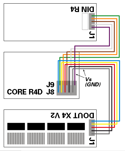
Connection to Core Module
Check the version of your Boards;
if you're using SmashTV's Core that's equipped with double rows, you can build a split-cable to connect J8/J9 to a DIN and a DOUT:
Connecting Input Devices
Connecting 32 buttons to a DINX4 Connecting 16 Rotary Ecnoders to the MIDIbox16E and other MIOS based controllers Connecting 16 Alps STEC16B03 Encoders to MIDIbox16E and other MIOS based controllers Connection Diagram for touch Sensors
Testing
Testing all pins
Regardless which MIDIbox you are planning to build, you can use the MIDIO128 application to test the digital inputs of the DIN module(s)
Once MIOS and the MIDIO128 application have been uploaded, each digital input will send a Note On event (pin 1-64) or Controller Event (pin 65-128) when a button is pressed (=0V at the digital input pin), and a Note Off event (pin 1-64) or Controller Event (pin 65-128) when the button is released (=5V at the digital input pin). Rotary encoders will send two Events (because they are connected to two pins) depending on the quadrature state.
Each pin will trigger an individual note/CC number. This is the second byte of a event. The first pin will send “90 30 7F” when pressed, and “90 30 00” when released. The last 128th pin will send “B0 4F 7F” when pressed, and “90 4F 00” when released. The MIDI events can be displayed with MIOS Studio or a MIDI monitor (e.g. MIDI-Ox) The MIDIO_OUT_ENTRY definitions in midio128_presets.inc help to map the pins to the events, the DIN DOUT pin list helps to map the pin numbers to shift register pins.
Testing Shift Register Connections
If the first input pin of the first shift register (74HC165) triggers all 128 Notes at once, there is propably a problem with the Shift or Register Clock line (SC/RC signal). Both signals are driven by the core module, and they are connected to all shift registers in order to scan the chain. If these signals are not connected, or if there is a short, the core will always “see” the first digital pin, and never the remaining pins of the chain.
If some of the last shift registers cannot be scanned, it is very likely that the SC/RC line is broken, that there is a bad soldering, or similar.
Such types of errors can be located with the srio_interconnection_test application, which can be found at the MIOS download page. Step by Step instructions for the testing procedure are described in the main.asm file
Check:
- the SC/RC output at the core module (J8/J9)
- the SC/RC input of each DINX4 module (J1/J2)
- the LD/CLK input of each 74HC165 (Pin #1 and Pin #2, see DINX4 schematic)
If you notice a short circuit (signals always 0V or 5V, or between these voltage levels), check the cables between the modules and especially your soldering at the bottom of the PCB. Consider also, that a PCB track could be broken or connected with another track (etching imperfection).
Connect each signle DINX4 module directly to the core in order to find the bad candidate(s).
If visual checks don't help to detect the short circuit, you could begin with a very drastic, but effective method: cut the failing track in the middle, and check if the short has disappeared. Cutting has to be repeated until you've found the cause for the failure.
Warning: Don't do this too early, this should be the last measure which normaly leads to success, but also to a bad looking PCB. After this procedure, you have to repair the track with some solder
Troubleshooting
Reference
home/mbhp/module/din.1228249534.txt.gz · Last modified: 2008/12/02 20:25 by Just Phil
Except where otherwise noted, content on this wiki is licensed under the following license: CC Attribution-Noncommercial-Share Alike 4.0 International
