Table of Contents
AOUT_4 module
Using the MAX525 DAC gives nice CVs. The circuit is designed with an improved output buffer. It's possible to switch the gain and and offset for different CV ranges.
Schematic
The DAC portion is essentially the same as the original version:

The gates were omitted. Normally RC1 can be used for two cascaded DACs.
The AOUTs each go through a buffer:
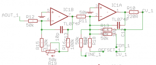
This is a dual inverting-opamp design. The first adjusts the scale of the CV. The second has extra mixer resistors to inject other CVs, such as a fixed offset and/or fine-tune control.
BOM v1.1
| Part | Value | Package | Description |
|---|---|---|---|
| C1 | 10u | E2,5-6 | POLARIZED Cap |
| C2 | 100n | C025-025×050 | CAPACITOR |
| C3 | 10u | E2,5-6 | POLARIZED Cap |
| C4 | 100n | C025-025×050 | CAPACITOR |
| C5 | 100n | C025-025×050 | CAPACITOR |
| C6 | 100n | C025-025×050 | CAPACITOR |
| C7 | 100n | C025-025×050 | CAPACITOR |
| C8 | 100n | C025-025×050 | CAPACITOR |
| C9 | 10u | E2,5-6 | POLARIZED CAP |
| C10 | 100n | C025-025×050 | CAPACITOR |
| C11 | 10n | C025-025×050 | CAPACITOR |
| C12 | 10p | C025-025×050 | CAPACITOR |
| C13 | 10p | C025-025×050 | CAPACITOR |
| C14 | 10p | C025-025×050 | CAPACITOR |
| C15 | 10p | C025-025×050 | CAPACITOR |
| C16 | 10p | C025-025×050 | CAPACITOR |
| C17 | 10p | C025-025×050 | CAPACITOR |
| C18 | 10p | C025-025×050 | CAPACITOR |
| C19 | 10p | C025-025×050 | CAPACITOR |
| C20 | 10n | C025-025×050 | CAPACITOR |
| C21 | 10u | E2,5-6 | POLARIZED |
| C22 | 100n | C025-025×050 | CAPACITOR |
| IC1 | TL074P | DIL14 | OPAMP |
| IC2 | TL074P | DIL14 | OPAMP |
| IC3 | MAX525 | DIL20_SML | DAC |
| IC4 | MAX6007* | LM4041A12DBZ | Vref |
| J1 | PINHD-2X54WALL | PINHEADER | |
| J2 | PINHD-2X54WALL | PINHEADER | |
| J3 | PINHD-2X54WALL | PINHEADER | |
| JP1 | PINHD-1X2SMALL | PINHEADER | |
| JP2 | PINHD-1X2SMALL | PINHEADER | |
| JP3 | PINHD-1X2SMALL | PINHEADER | |
| JP6 | PINHD-1X2SMALL | PINHEADER | |
| JP7 | PINHD-1X2SMALL | PINHEADER | |
| JP8 | PINHD-1X2SMALL | PINHEADER | |
| JP9 | PINHD-1X2SMALL | PINHEADER | |
| JP10 | PINHD-1X3SMALL | PINHEADER | |
| JP11 | PINHD-1X3SMALL | PINHEADER | |
| JP12 | PINHD-1X3SMALL | PINHEADER | |
| JP13 | PINHD-1X3SMALL | PINHEADER | |
| JP14 | PINHD-1X3SMALL | PINHEADER | |
| JP15 | PINHD-1X3SMALL | PINHEADER | |
| JP16 | PINHD-1X3SMALL | PINHEADER | |
| JP17 | PINHD-1X3SMALL | PINHEADER | |
| L1 | BEAD | 5MM | INDUCTOR |
| L2 | BEAD | 5MM | INDUCTOR |
| R1 | 1k | 0204/7 | RESISTOR |
| R3 | 1k | 0204/7 | RESISTOR |
| R10 | 220R | 0204/7 | RESISTOR |
| R11 | 50k | 0204/7 | RESISTOR |
| R12 | 50k | 0204/7 | RESISTOR |
| R13 | 50k | 0204/7 | RESISTOR |
| R14 | 50k | 0204/7 | RESISTOR |
| R15 | 130k | 0207/2V | RESISTOR |
| R16 | 100k | 0204/7 | RESISTOR |
| R17 | 50k | 0204/7 | RESISTOR |
| R18 | 50k | 0204/7 | RESISTOR |
| R19 | 50k | B64Y | trim pot |
| R20 | 220R | 0204/7 | RESISTOR |
| R21 | 50k | 0204/12_ANDY | RESISTOR |
| R22 | 50k | 0204/9_ANDY | RESISTOR |
| R23 | 50k | 0204/7 | RESISTOR |
| R24 | 50k | 0204/7 | RESISTOR |
| R25 | 130k | 0207/2V | RESISTOR |
| R26 | 100k | 0204/7 | RESISTOR |
| R27 | 50k | 0204/12_ANDY | RESISTOR |
| R28 | 50k | 0204/7 | RESISTOR |
| R29 | 50k | B64Y | trim pot |
| R30 | 220R | 0204/7 | RESISTOR |
| R31 | 50k | 0204/9_ANDY | RESISTOR |
| R32 | 50k | 0204/9_ANDY | RESISTOR |
| R33 | 50k | 0204/7 | RESISTOR |
| R34 | 50k | 0204/7 | RESISTOR |
| R35 | 130k | 0207/2V | RESISTOR |
| R36 | 100k | 0207/2V | RESISTOR |
| R37 | 50k | 0204/7 | RESISTOR |
| R38 | 50k | 0204/7 | RESISTOR |
| R39 | 50k | B64Y | trim pot |
| R40 | 220R | 0204/7 | RESISTOR |
| R41 | 50k | 0204/12_ANDY | RESISTOR |
| R42 | 50k | 0204/7 | RESISTOR |
| R43 | 50k | 0204/7 | RESISTOR |
| R44 | 50k | 0204/7 | RESISTOR |
| R45 | 130k | 0204/7 | RESISTOR |
| R46 | 100k | 0204/7 | RESISTOR |
| R47 | 50k | 0204/7 | RESISTOR |
| R48 | 50k | 0204/7 | RESISTOR |
| R49 | 50k | B64Y | trim pot |
| RC1_RC2 | SJ2W | Jumper | (normally as RC1) |
| VR1 | VOLTAGE reg | (optional) |
Versions
v1.1: first release.
Assembly
The clearance with the common 3296 series trimpots is quite tight! Although everything does fit, you may wish to place the trimpots in before the surrounding resistors. The resistors could even go on the back of the board, as long as you don't melt the trimmer housings too much. There are smaller trimmers available, but they seem to be quite pricey.
The 50k value for most resistors is not too important. 47k will work fine.
For best results, get 0.1% resistors or hand-match R11/13/14/17/18, R21/23/24/27/28 and so on.
Headers and jumpers
J1 is a normal Eurorack-style power header. Stripe = -12V J2 matches a Core J19 header. RC1/RC2 solder jumper: connect only one (RC1 normally) to the centre pad J3 can cascade additional modules. Two can use the same latch (RC1 or RC2).
JP1 is intended as a connector to other boards or for SIP connectors pin order from the part designator: 0V|3v3|0V|-12V|0V|+12V
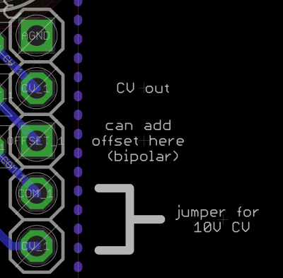
JP14/15/16/17: the square pin can be connected to an offset voltage for fine tuning. This will need some reference to the +/-12V rails.
JP6/7/8/9:
Interconnection to Core
As noted above.
License
Currently the design is © 2018 antilog devices with all rights reserved; all documentation is CC BY-NC-SA 3.0.