Table of Contents
'ELO
Illuminated encoders and OLEDs mounted at 45 degrees. Optional touch sensors.
Hardware mapping
Schematic
WS2812 LEDs are arranged in a snake pattern entering at J1 and exiting at J2. R1 should be installed as a resistor 220-470R for the first module only and as a wire link for any subsequent WS2812 modules. There are pads for RC termination, which shouldn't be required.
A DIN chain scans the encoders and touch sensors coming in on J3 and out on J4. The encoders are assigned in columns to a 165 shift register with the top position using D0/D1, the second D1/D2, etc. Note that the clear-shaft encoders have the pin directions swapped; this should be taken into account in an MB_NG file. In theory the SRIO chain could be extended from J4.
There are 16 separate touch sensor circuits as shown (circuit design adapted from Talking Electronics):
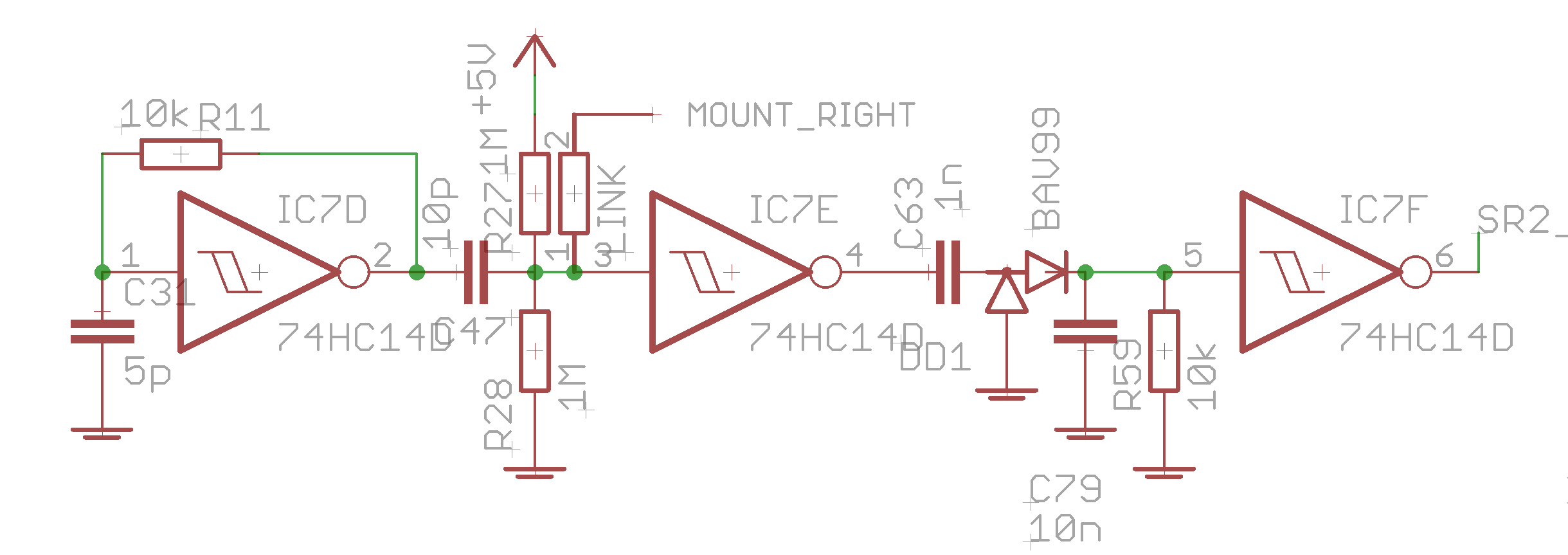
The first inverter comprises an oscillator feeding into another inverter. By touching the “LINK” part, the capacitance increases. The third inverter forms a comparator. In the normal state, the oscillator keeps the gate output low. When touched, the oscillator will “bleed” through and set the gate high. The actual part values may need adjusting to suit your own body/environment. To use plates mounted onto the encoder bodies, solder a wire link across the TS parts as noted. To use other metal pieces (e.g. an external keyboard), connect a wire to the pads adjacent to surface-mount parts.
- If touch sensors are not required, pins 9/10 of IC2 and IC5 can be bridged and the 165 chips/resistor networks omitted (this will obviously change the addressing of encoders!).
- If the 165 chips are installed but no touch sensors are used, then the resistor networks must also be installed.
- If touch sensors are used, then RN2/5 should be omitted. The inverter gates ensure a defined logic level.
The OLED displays are connected as follows:
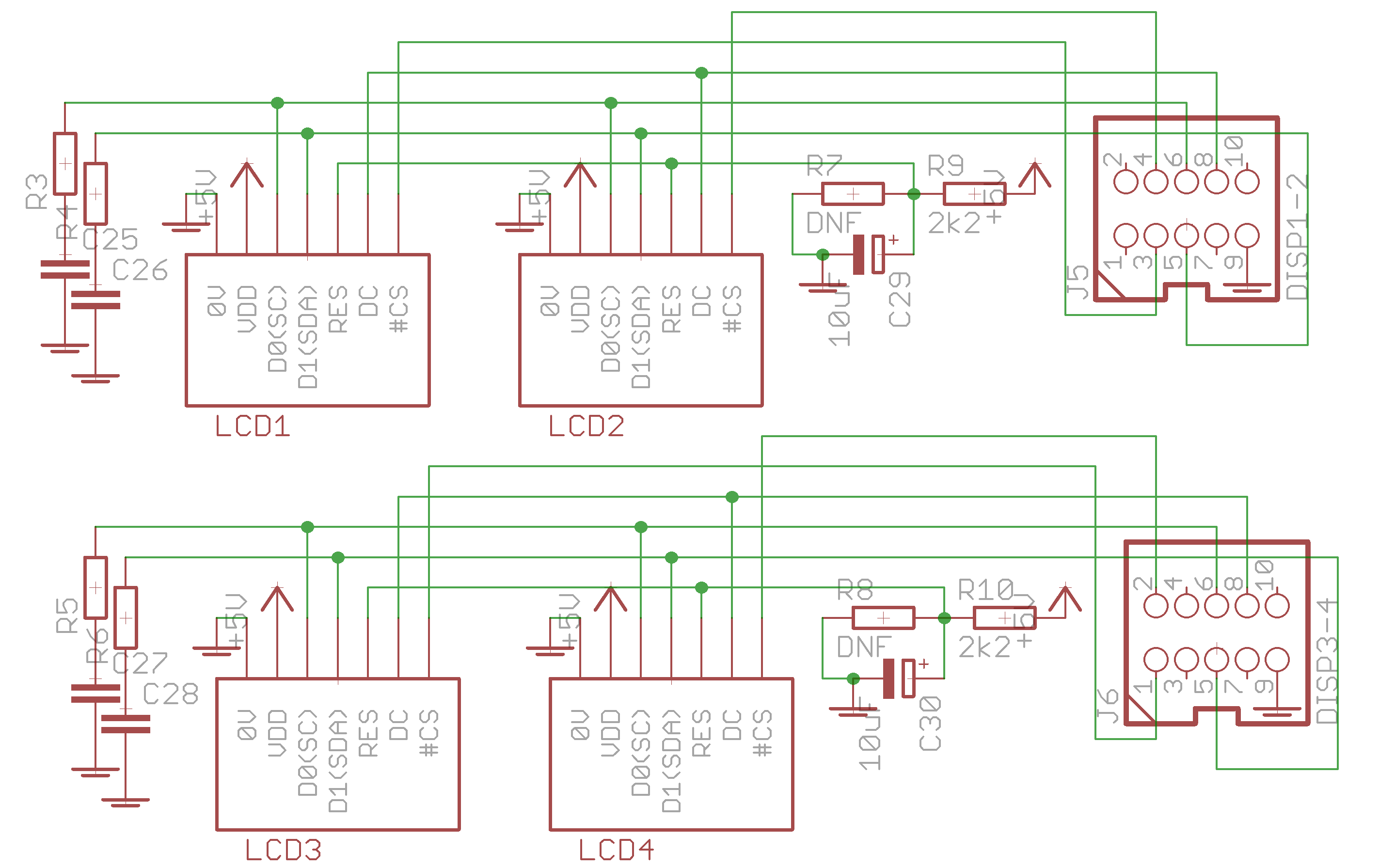
The reset circuits R9/R10/C29/C30 should be installed. The termination circuits R3-6/C25-28 shouldn't be required. When wiring ribbon cables, the end attached to the ELO board should have two IDCs on it; there is no connection on the PCB for the clock/data etc. lines between the two pairs of displays.
+5V Power enters through J7 and D1. There is no connection to +5V on other headers, apart from J4 to potentially drive SRIO modules.
BOM v1.0
| Type | Part | Value | Device |
|---|---|---|---|
| Caps | C1 | 10—100uF | CPOL-EU-1 |
| C2 | 100n | C1206 | |
| C3 | 100n | C1206 | |
| C4 | 100n | C1206 | |
| C5 | 100n | C1206 | |
| C6 | 100n | C1206 | |
| C7 | 100n | C1206 | |
| C8 | 100n | C1206 | |
| C9 | 100n | C1206 | |
| C10 | 100n | C1206 | |
| C11 | 100n | C1206 | |
| C12 | 100n | C1206 | |
| C13 | 100n | C1206 | |
| C14 | 100n | C1206 | |
| C15 | 100n | C1206 | |
| C16 | 100n | C1206 | |
| C17 | 100n | C1206 | |
| C18 | DNF | ||
| C19 | 100n | C1206 | |
| C20 | 100n | C1206 | |
| C21 | 100n | C1206 | |
| C22 | 100n | C1206 | |
| C23 | 100n | C1206 | |
| C24 | 100n | C1206 | |
| C25 | DNF | ||
| C26 | DNF | ||
| C27 | DNF | ||
| C28 | DNF | ||
| C29 | 10uF | CPOL-EUE2.5-5 | |
| C30 | 10uF | CPOL-EUE2.5-5 | |
| C31 | 5p | C-EUC1206 | |
| C32 | 5p | C-EUC1206 | |
| C33 | 5p | C-EUC1206 | |
| C34 | 5p | C-EUC1206 | |
| C35 | 5p | C-EUC1206 | |
| C36 | 5p | C-EUC1206 | |
| C37 | 5p | C-EUC1206 | |
| C38 | 5p | C-EUC1206 | |
| C39 | 5p | C-EUC1206 | |
| C40 | 5p | C-EUC1206 | |
| C41 | 5p | C-EUC1206 | |
| C42 | 5p | C-EUC1206 | |
| C43 | 5p | C-EUC1206 | |
| C44 | 5p | C-EUC1206 | |
| C45 | 5p | C-EUC1206 | |
| C46 | 5p | C-EUC1206 | |
| C47 | 10p | C-EUC1206 | |
| C48 | 10p | C-EUC1206 | |
| C49 | 10p | C-EUC1206 | |
| C50 | 10p | C-EUC1206 | |
| C51 | 10p | C-EUC1206 | |
| C52 | 10p | C-EUC1206 | |
| C53 | 10p | C-EUC1206 | |
| C54 | 10p | C-EUC1206 | |
| C55 | 10p | C-EUC1206 | |
| C56 | 10p | C-EUC1206 | |
| C57 | 10p | C-EUC1206 | |
| C58 | 10p | C-EUC1206 | |
| C59 | 10p | C-EUC1206 | |
| C60 | 10p | C-EUC1206 | |
| C61 | 10p | C-EUC1206 | |
| C62 | 10p | C-EUC1206 | |
| C63 | 1n | C-EUC1206 | |
| C64 | 1n | C-EUC1206 | |
| C65 | 1n | C-EUC1206 | |
| C66 | 1n | C-EUC1206 | |
| C67 | 1n | C-EUC1206 | |
| C68 | 1n | C-EUC1206 | |
| C69 | 1n | C-EUC1206 | |
| C70 | 1n | C-EUC1206 | |
| C71 | 1n | C-EUC1206 | |
| C72 | 1n | C-EUC1206 | |
| C73 | 1n | C-EUC1206 | |
| C74 | 1n | C-EUC1206 | |
| C75 | 1n | C-EUC1206 | |
| C76 | 1n | C-EUC1206 | |
| C77 | 1n | C-EUC1206 | |
| C78 | 1n | C-EUC1206 | |
| C79 | 10n | C-EUC1206 | |
| C80 | 10n | C-EUC1206 | |
| C81 | 10n | C-EUC1206 | |
| C82 | 10n | C-EUC1206 | |
| C83 | 10n | C-EUC1206 | |
| C84 | 10n | C-EUC1206 | |
| C85 | 10n | C-EUC1206 | |
| C86 | 10n | C-EUC1206 | |
| C87 | 10n | C-EUC1206 | |
| C88 | 10n | C-EUC1206 | |
| C89 | 10n | C-EUC1206 | |
| C90 | 10n | C-EUC1206 | |
| C91 | 10n | C-EUC1206 | |
| C92 | 10n | C-EUC1206 | |
| C93 | 10n | C-EUC1206 | |
| C94 | 10n | C-EUC1206 | |
| C95 | 100n | C1206 | |
| C96 | 100n | C1206 | |
| C97 | 100n | C1206 | |
| C98 | 100n | C1206 | |
| C99 | 100n | C1206 | |
| C100 | 100n | C1206 | |
| C101 | 100n | C1206 | |
| C102 | 100n | C1206 | |
| Diodes | D1 | 1N5817 | 1N5817-B |
| DD1 | BAV99 | BAV99 | |
| DD2 | BAV99 | BAV99 | |
| DD3 | BAV99 | BAV99 | |
| DD4 | BAV99 | BAV99 | |
| DD5 | BAV99 | BAV99 | |
| DD6 | BAV99 | BAV99 | |
| DD7 | BAV99 | BAV99 | |
| DD8 | BAV99 | BAV99 | |
| DD9 | BAV99 | BAV99 | |
| DD10 | BAV99 | BAV99 | |
| DD11 | BAV99 | BAV99 | |
| DD12 | BAV99 | BAV99 | |
| DD13 | BAV99 | BAV99 | |
| DD14 | BAV99 | BAV99 | |
| DD15 | BAV99 | BAV99 | |
| DD16 | BAV99 | BAV99 | |
| Encoders | EN1 | ENCODER_NO_SWITCHSW | ENCODER_NO_SWITCH |
| EN2 | ENCODER_NO_SWITCHSW | ENCODER_NO_SWITCH | |
| EN3 | ENCODER_NO_SWITCHSW | ENCODER_NO_SWITCH | |
| EN4 | ENCODER_NO_SWITCHSW | ENCODER_NO_SWITCH | |
| EN5 | ENCODER_NO_SWITCHSW | ENCODER_NO_SWITCH | |
| EN6 | ENCODER_NO_SWITCHSW | ENCODER_NO_SWITCH | |
| EN7 | ENCODER_NO_SWITCHSW | ENCODER_NO_SWITCH | |
| EN8 | ENCODER_NO_SWITCHSW | ENCODER_NO_SWITCH | |
| EN9 | ENCODER_NO_SWITCHSW | ENCODER_NO_SWITCH | |
| EN10 | ENCODER_NO_SWITCHSW | ENCODER_NO_SWITCH | |
| EN11 | ENCODER_NO_SWITCHSW | ENCODER_NO_SWITCH | |
| EN12 | ENCODER_NO_SWITCHSW | ENCODER_NO_SWITCH | |
| EN13 | ENCODER_NO_SWITCHSW | ENCODER_NO_SWITCH | |
| EN14 | ENCODER_NO_SWITCHSW | ENCODER_NO_SWITCH | |
| EN15 | ENCODER_NO_SWITCHSW | ENCODER_NO_SWITCH | |
| EN16 | ENCODER_NO_SWITCHSW | ENCODER_NO_SWITCH | |
| ICs | IC1 | 74HC165D | SOIC16 |
| IC2 | 74HC165D | SOIC16 | |
| IC3 | 74HC165D | SOIC16 | |
| IC4 | 74HC165D | SOIC16 | |
| IC5 | 74HC165D | SOIC16 | |
| IC6 | 74HC165D | SOIC16 | |
| IC7 | 74HC14D | SOIC14 | |
| IC8 | 74HC14D | SOIC14 | |
| IC9 | 74HC14D | SOIC14 | |
| IC10 | 74HC14D | SOIC14 | |
| IC11 | 74HC14D | SOIC14 | |
| IC12 | 74HC14D | SOIC14 | |
| IC13 | 74HC14D | SOIC14 | |
| IC14 | 74HC14D | SOIC14 | |
| Headers | J1 | WS2812 | IN |
| J2 | WS2812 | OUT | |
| J3 | SRIO IN | PAK100/2500-10 | |
| J4 | SRIO OUT | PAK100/2500-10 | |
| J5 | DISP1-2 | PINHD-2X54WALL | |
| J6 | DISP3-4 | PINHD-2X54WALL | |
| J7 | +5V | 22-23-2031 | |
| Displays | LCD1 | 0.96_OLED | LCD_OLED_0.96_PINS |
| LCD2 | 0.96_OLED | LCD_OLED_0.96_PINS | |
| LCD3 | 0.96_OLED | LCD_OLED_0.96_PINS | |
| LCD4 | 0.96_OLED | LCD_OLED_0.96_PINS | |
| LEDs | LED1 | WS2812B | WS2812B |
| LED2 | WS2812B | WS2812B | |
| LED3 | WS2812B | WS2812B | |
| LED4 | WS2812B | WS2812B | |
| LED5 | WS2812B | WS2812B | |
| LED6 | WS2812B | WS2812B | |
| LED7 | WS2812B | WS2812B | |
| LED8 | WS2812B | WS2812B | |
| LED9 | WS2812B | WS2812B | |
| LED10 | WS2812B | WS2812B | |
| LED11 | WS2812B | WS2812B | |
| LED12 | WS2812B | WS2812B | |
| LED13 | WS2812B | WS2812B | |
| LED14 | WS2812B | WS2812B | |
| LED15 | WS2812B | WS2812B | |
| LED16 | WS2812B | WS2812B | |
| Resistors | R1 | 220-470R | R-EU_0204/7 |
| R2 | DNF | ||
| R3 | DNF | ||
| R4 | DNF | ||
| R5 | DNF | ||
| R6 | DNF | ||
| R7 | DNF | ||
| R8 | DNF | ||
| R9 | 2k2 | R-EU_0204/7 | |
| R10 | 2k2 | R-EU_0204/7 | |
| R11 | 10k | R-EU_R1206 | |
| R12 | 10k | R-EU_R1206 | |
| R13 | 10k | R-EU_R1206 | |
| R14 | 10k | R-EU_R1206 | |
| R15 | 10k | R-EU_R1206 | |
| R16 | 10k | R-EU_R1206 | |
| R17 | 10k | R-EU_R1206 | |
| R18 | 10k | R-EU_R1206 | |
| R19 | 10k | R-EU_R1206 | |
| R20 | 10k | R-EU_R1206 | |
| R21 | 10k | R-EU_R1206 | |
| R22 | 10k | R-EU_R1206 | |
| R23 | 10k | R-EU_R1206 | |
| R24 | 10k | R-EU_R1206 | |
| R25 | 10k | R-EU_R1206 | |
| R26 | 10k | R-EU_R1206 | |
| R27 | 1M | R-EU_R1206 | |
| R28 | 1M | R-EU_R1206 | |
| R29 | 1M | R-EU_R1206 | |
| R30 | 1M | R-EU_R1206 | |
| R31 | 1M | R-EU_R1206 | |
| R32 | 1M | R-EU_R1206 | |
| R33 | 1M | R-EU_R1206 | |
| R34 | 1M | R-EU_R1206 | |
| R35 | 1M | R-EU_R1206 | |
| R36 | 1M | R-EU_R1206 | |
| R37 | 1M | R-EU_R1206 | |
| R38 | 1M | R-EU_R1206 | |
| R39 | 1M | R-EU_R1206 | |
| R40 | 1M | R-EU_R1206 | |
| R41 | 1M | R-EU_R1206 | |
| R42 | 1M | R-EU_R1206 | |
| R43 | 1M | R-EU_R1206 | |
| R44 | 1M | R-EU_R1206 | |
| R45 | 1M | R-EU_R1206 | |
| R46 | 1M | R-EU_R1206 | |
| R47 | 1M | R-EU_R1206 | |
| R48 | 1M | R-EU_R1206 | |
| R49 | 1M | R-EU_R1206 | |
| R50 | 1M | R-EU_R1206 | |
| R51 | 1M | R-EU_R1206 | |
| R52 | 1M | R-EU_R1206 | |
| R53 | 1M | R-EU_R1206 | |
| R54 | 1M | R-EU_R1206 | |
| R55 | 1M | R-EU_R1206 | |
| R56 | 1M | R-EU_R1206 | |
| R57 | 1M | R-EU_R1206 | |
| R58 | 1M | R-EU_R1206 | |
| R59 | 10K | R-EU_R1206 | |
| R60 | 10K | R-EU_R1206 | |
| R61 | 10K | R-EU_R1206 | |
| R62 | 10K | R-EU_R1206 | |
| R63 | 10K | R-EU_R1206 | |
| R64 | 10K | R-EU_R1206 | |
| R65 | 10K | R-EU_R1206 | |
| R66 | 10K | R-EU_R1206 | |
| R67 | 10K | R-EU_R1206 | |
| R68 | 10K | R-EU_R1206 | |
| R69 | 10K | R-EU_R1206 | |
| R70 | 10K | R-EU_R1206 | |
| R71 | 10K | R-EU_R1206 | |
| R72 | 10K | R-EU_R1206 | |
| R73 | 10K | R-EU_R1206 | |
| R74 | 10K | R-EU_R1206 | |
| Resistor networks | RN1 | 10k | 652-4816P-T2LF-10K |
| RN2 | DNF/see notes | ||
| RN3 | 10k | 652-4816P-T2LF-10K | |
| RN4 | 10k | 652-4816P-T2LF-10K | |
| RN5 | DNF/see notes | ||
| RN6 | 10k | 652-4816P-T2LF-10K | |
| Touch sensors | TS1 | R-EU_TS | 0204TS |
| TS2 | R-EU_TS | 0204TS | |
| TS3 | R-EU_TS | 0204TS | |
| TS4 | R-EU_TS | 0204TS | |
| TS5 | R-EU_TS | 0204TS | |
| TS6 | R-EU_TS | 0204TS | |
| TS7 | R-EU_TS | 0204TS | |
| TS8 | R-EU_TS | 0204TS | |
| TS9 | R-EU_TS | 0204TS | |
| TS10 | R-EU_TS | 0204TS | |
| TS11 | R-EU_TS | 0204TS | |
| TS12 | R-EU_TS | 0204TS | |
| TS13 | R-EU_TS | 0204TS | |
| TS14 | R-EU_TS | 0204TS | |
| TS15 | R-EU_TS | 0204TS | |
| TS16 | R-EU_TS | 0204TS |
Versions
v1.0: first release.
Assembly
If using touch sensors, install the SMT parts first. Capacitor pads have rounded corners and there is a silkscreen line along the longer edge to help orient the parts. See above for how to connect TS parts (normally a wire link).
The WS2812 LEDs and associated caps should come next, followed by the SMT shift registers and resistor networks. See above for notes on the RNs.
Here it is a good idea to test the LED functions before overlaying the encoders.
The encoders can then be installed over the LEDs. They need to be raised above the LED (e.g. using a spacer piece of 2mm) so the shaft turns freely, and the mounting legs should be straightened for a secure connection.
OLED displays should go in last. As they mount over the touch sensors, it would be smart to test the touch sensor operation before they are placed.
Example usage:
Interconnection to Core
- J1 to J4B (I2C)
- J3 to J89 (SRIO)
- J5/J6 to J15 or equivalent. The ribbon cable should have two IDCs on the ELO end, one for J5 and one for J6.
- J7 +5V as noted.
Dimensions

License
Currently the design is © 2018 antilog devices with all rights reserved; all documentation is CC BY-NC-SA 3.0.