Table of Contents
fnpSID Module
This page is dedicated to Flexinoodle's & nILS' stereo USB implementation MIDIBox SID v2. All information present on and files linked to from this site are
© 2009 nILS Podewski. Free for private, non-commercial use. All other rights reserved.

PCB overview
The PCB is 6.3 x 3.9 inches (16 x 10 cm) (Eurocard) and looks like this:
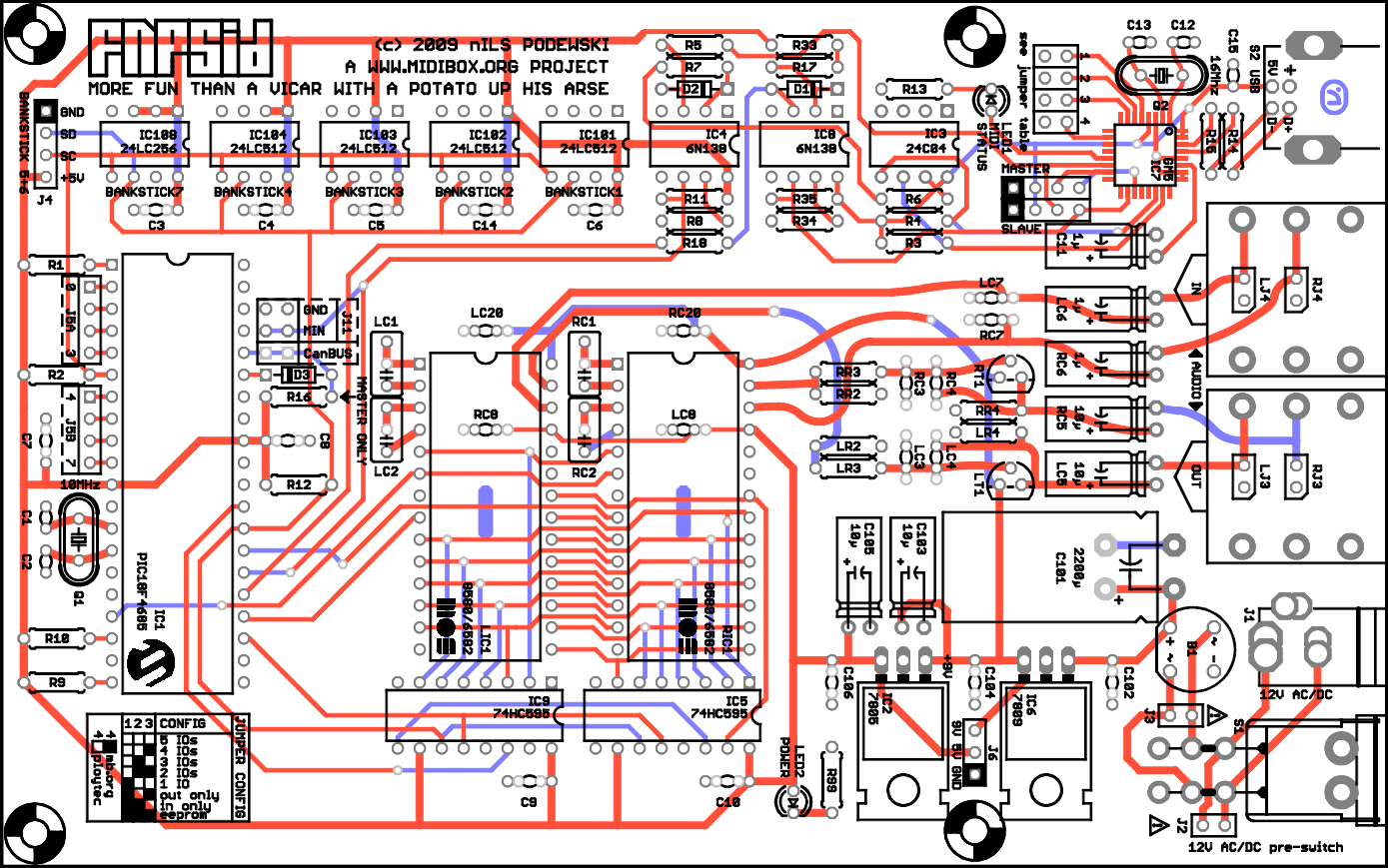
(click for full size)
A .pdf version is available here
Connectors
| Name | Number of pins | Description |
| S2 | 1 | USB connector |
| S1 | 1 | On/Off Switch |
| J2 | 1 | 12V input (AC/DC) |
| In | 1 | 1/4“ Stereo Jack for audio input |
| Out | 1 | 1/4” Stereo Jack for audio output |
| J3 | 1 | 12V power output (after the switch, you can hook a second fnpSID or other hardware up to switch them on/off with this pcb) |
| J2 | 1 | 12V power source (before the switch - careful, this header is always hot. DO NOT MOUNT this header unless you really know why you are doing it.) |
| J11 | 1 | CANbus connection to connect more fnpSID PCBs or another Core/SID module combo |
| J4 | 2 | Header for adding external banksticks #5/#6 (see Core:J4 pinout) |
Part list / BOM
FLEXI_ATTENTION: Caps need info on lead spacing
| Part | Value | Count | Footprint/ lead spacing | Part # |
| SID | 6582/8580 | 2 | - | LIC1,RIC1 |
| GM5 | GM5 | 1 | TQFP32 | IC7 |
| PIC18F4685-I/P | PIC18F4685 | 1 | DIP40 | IC1 |
| Shift Register | 74HC595 | 2 | DIP 16 | IC5,IC9 |
| Optocoupler | 6N138 | 2 | DIP 8 | IC4,IC8 |
| Voltage Regulator TO220 | 7805 | 1 | - | IC2 |
| Voltage Regulator TO220 | 7809 | 1 | - | IC6 |
| EEPROM | 24C04 | 1 | DIP8 | IC3 |
| EEPROM | 24LC512 | 4 | DIP8 | IC101 - IC104 |
| EEPROM | 24LC256 | 1 | DIP8 | IC108 |
| Crystal | 10.0 MHz | 1 | HC49 | Q1 |
| Crystal | 16.0 MHz | 1 | HC49 | Q2 |
| LED 3mm | - | 2 | - | LED1,LED2 |
| Diode | 1N4148 | 3 | - | D1 – D3 |
| Bridge Rectifier | B40C800 | 1 | - | B1 |
| Transistor TO92 | BC547C | 2 | - | LT1,RT1 |
| Ceramic Capacitor | 470p | 2 | - | LC4,RC4 |
| Ceramic Capacitor | 22p | 2 | - | C12, C13 |
| Ceramic Capacitor | 33p | 2 | - | C1, C2 |
| Electrolytic Capacitor | 10µ | 4 | - | C103, C105, LC5, RC5 |
| Electrolytic Capacitor | 2200µ | 1 | - | C101 |
| Electrolytic Capacitor | 1µ | 3 | - | C11, LC6, RC6 |
| Electrolytic Capacitor | 10µ | 4 | - | C103, C105, LC5, RC5 |
| Polyester Film Capacitor (Xicon) | 22n | 4 | - | LC1, LC2, RC1, RC2 |
| Capacitor | 330n | 1 | - | C102 |
| Capacitor | 1n | 4 | - | LC3, LC7, RC3, RC7 |
| Capacitor | 100n | 15 | - | C3 - C10, C14, C104, C106, LC8, LC20, RC8, RC20 |
| Resistor | 1k | 9 | - | LR2, LR4, R2, R3, R4, R12, R16, RR2, RR4 |
| Resistor | 1k2 | 2 | - | R11, R35 |
| Resistor | 5k6 | 2 | - | R8, R34 |
| Resistor | 10k | 4 | - | LR3, R9, R10, RR3 |
| Resistor | 27 | 2 | - | R14, R15 |
| Resistor | 100 | 1 | - | R1 |
| Resistor | 220 | 8 | - | R5, R6, R7, R13, R17, R18, R33, R99 |
| DPDT Switch | - | 1 | - | S1 |
| 1/4“ switched stereo socket | - | 2 | - | IN_L,OUT_L |
| USB type B socket | USB-B | 1 | - | S2 |
| Pin Header | 40 | 1 | - | |
| 2.1/2.5mm DC power socket | PJ-202AH | 1 | - | J1 |
Hardware Options
Parts with multiple footprints
PLACEHOLDER
Pick your poison
There are multiple hardware options for the fnpSID
1. Single PCB StereoSID
This option is the most basic and will give you a single MBSID with stereo capabilities
2. Dual PCB QuadSID MIDI linked
This option will give you two of the basic stereo MBSID as listed above both with there own MIDI port on the computer
In this configuration you will use the master slave jumpers and power can be taken from j3
3. Dual PCB QuadSID CANbus linked
This option uses the CAN bus and as such has the option to use super poly mode and shared banksticks when combined
In this configuartion you will use the canbus jumper and power can be taken from j3
Assembly Guide
The following sections will guide you through the entire process of getting your fnpSID up and running. Take one step at a time and you'll be done in a jiffy.
1. Soldering
1. First solder in the GM5 chip (It's beyond the scope of this page to give tutorials on SMD. Needless to say check YOUtube for vids and check out Flexi's GM5 notes )
2. Solder in all the resistors (Solder the resistor “suited” meaning all in the same direction - because believe me it does aid in diagnosing any issues later)
3. Solder in the diodes (Be sure you have them in the right direction: black line on the diode goes to the screen print line on the PCB)
4. Solder in the capacitors but leave the electrolytics until later (This is purely a height thing it makes it easier to solder other components so leave the big ones for now)
5. Solder in the transistors (Be sure to line them up correctly)
6. Solder in the bridge rectifier (Make sure the + leg goes to the + screen printed on the PCB)
6. Solder in the two LEDs (The screen print triangle on the PCB points to the cathode which is the short leg)
7. Solder in the two voltage regulators (Make sure you bend the legs before soldering and dont worry too much if the hole doesn't line up with the board as you won't need to screw them to the board)
8. Solder an 8-pin DIL header into the GM5 jumper (to the left of the GM5 and place jumpers all the way along )
9. Solder a SIL header into the MASTER jumper (We will discuss the slave header in the slave soldering addendum later)
10. Solder in the GM5 crystal Q2 (Make sure you use the 16mhz crystal)
11. Solder the core crystal Q1 (Make sure you use the 10mhz crystal)
12. Solder in all the IC sockets (You can work these out for yourself, make sure the mark goes on the right side)
13. Solder in the electrolytic capacitors (Make sure the polarity is correct - the line on the capacitor is the negative side. Again, it helps to bend the pins before soldering the capacitor)
14. Solder in your external connectors (USB/Power/Switch/Audio jacks in that order)
15. Thats all the soldering done time to move on to testing. Do not stuff any of the ICs yet.
2. Testing
1. Turn the power switch off (down position)
2. Plug in the wallwart.
3. If in step 4 the power LED (LED2) does not light up or you get funny smells or magic smoke unplug the PSU immediately.
4. Turn the power switch on.
5. Whilst powered check the voltages across these pins:
| Pins | Voltage |
| IC1:11(Vcc) - IC1:12(Vss) | 5V |
| IC1:32(Vcc) - IC1:31(Vss) | 5V |
| LIC1:25(Vcc) - LIC1:7(Vcc) | 5V |
| RIC1:25(Vcc) - RIC1:7(Vcc) | 5V |
| LIC1:28(Vdd) - LIC1:28(Vss) | 9V |
| RIC1:28(Vdd) - RIC1:28(Vss) | 9V |
If all the voltages are good, continue - let's finish up.
Finishing up
1. Install the PIC into IC1 (Make sure the notch at the end of the PIC lines up with the screen printed notch on the PCB)
2. Install the 74HC595s into IC9,IC5 (Again line up the notch with the screen print notch)
3. Install the 24C04 into IC3 (Hmmm something about notches i think ? )
4. Install the 6N138's into IC4,IC8 (take a guess)
5. Install the 24LC512 into IC101 - 104 (Meh)
6. Install the 24LC256 into IC108 (Yup)
7. Install the SIDs into LC8,RC8 (Yay)
8. Plug in the USB cable and connect to your computer (The computer should find the GM5 and use the OS's built in driver)
9. Load MIOS Studio and connect its output to GM5 port 1 and its input to GM5 port 1 (Just click on routing and its pretty self explanatory)
10. Turn on MIOS Studio MIDI monitors and then turn on your fnpSID (You should see a couple of SYSEX commands received by MIOS Studio)
11. Upload the latest firmware (use the setup_8580.hex) to the fnpSID (you can find instructions on how to do this atucapps.de )
12. Show the MIOS Studio virtual keyboard and play a few keys (You should hear the default patch playing from the fnpSID)
13. Turn the fnp off then back on (you should hear a bleep for each bankstick installed)
14. Screw the rear panel onto the two side pieces of your enclosure and then slide in the top and bottom panels (Makes life easier doing the back panel first)
15. Slide your fnpSID board into the lowest slot in the case and then screw on the front panel (Don't forget to remove the audio sockets panel nuts and refit them when finished)
16. Install the SID soundbanks (More info on this later)
17. Go play at being a SID superstar
Order lists
Join the group buy bitch heheheheh yep this is a placeholder
FAQ - Frequently Asked Questions
FLEXI_ATTENTION: Needs info on missing headers and why they are missing.
Q: There are no ground connections in the pictures. Why?
A: The ground connections are on the bottom copper plane, which isn't visible in the pictures for easier reading.
Q: Can I have the .brd or .sch file?
A: No.
Q: Why can't I have the .brd or .sch file?
A: Because nILS says so.
Q: What does “fnp” stand for?
A: Flexinoodle nILS Podewski
Q: can I haz cheezburger?
A: Hmmmm let me think hmmmm erm NO
Q: I am a vicar with a potato up my arse, and this is not more fun. Can I haz refund?
A: If you can prove being a vicar AND provide photos of the potato up your arse, yes.
Flexi's GM5 Notes
Ok, when I started building the prototype of the fnpSID, I hadn't actually soldered for about 4 years
I tried every possible method I had seen to try and solder this chip and was totally convinced that - you know what - “I just couldn't solder anymore”.
So, after an hour of solidly frying the chip with the iron at 425 degrees and finally managing to get some solder to at least heat up and solder the legs nILS told me to solder in some components to see if it still worked. Needless to say I didn't hold out high hopes. Anyway, when I tried to solder in the first resistor it was all the same: “I just couldn't solder anymore”
Very frustrated I took a break and then checked the tip of my iron. Yes, the tip that nILS and I had chosen for the iron was the wrong one, even though I had checked with the supplier many times to make sure. The tip had overheated, pitted, blackened and was basically a horrific mess. I changed the tip back to the one that came with the iron (too big but what the hey).
About two minutes later I had soldered all the needed components to test and hey, guess what? Yep, that's right the GM5 worked perfectly. The thing to take from this story is this
1. Always check ya bloomin tools
2. Dont be scared of soldering the GM5 because if a gimpazoid newb like me can solder it after an hour of frying and not kill it, ANYBODY CAN SOLDER IT
- Flexinoodle
Wilba's fnpSID Notes
1. GM5 is easy to solder, read the SMD soldering tutorials and don't forget to use flux and solder wick! Soaking up excess solder is easier if you add some more flux.
2. It is easier to work with the board if you put some long screws or long spacers through the mount holes so it can stand above the work surface. Then you can place parts with long leads (i.e. resistors and capacitors) and cut the leads until after soldering.
3. After inserting all the resistors, you can flip the board over (use some card to stop resistors falling out) and solder all at once.
4. Lightly solder one top-side pad of capacitors and other small parts to hold them in place, then flip the board over and solder all at once.
5. Where #4 cannot be done (sockets, etc.), you can hold part in place by carrying a blob of solder on your iron to the pad while you hold the part in place with your other hand. The addition of flux to the pad makes this a lot easier. Don't forget to come back and properly solder this pad after you solder the other pads.
6. If you think your kit is missing some parts, check they didn't fall on the floor before complaining to nILS.
7. If you are looking for J15 on the PCB, it's located right next to J8/J9.
8. If you are looking for J8/J9 on the PCB, it's located right next to J15.
- Wilba