Table of Contents
KiCAD, An Open-Source Alternative to Eagle for PCB Design
1. Introduction
KiCAD is a Open Source Computer Assisted Drawing (CAD) software for designing Printed Circuit Boards (PCBs) from Schematics to Gerber Files. Its features have been enhanced through heavy development by CERN and the community. It supports up to 32 layers and has no limitation on the size of the PCB.
You can find the official website here : http://kicad-pcb.org/
2. Installation
First, download the correct installer for your operating system at
http://kicad-pcb.org/download/
Follow the instructions to get the program installed
3. Getting Started
The basic workflow in Kicad is split into 4 parts :
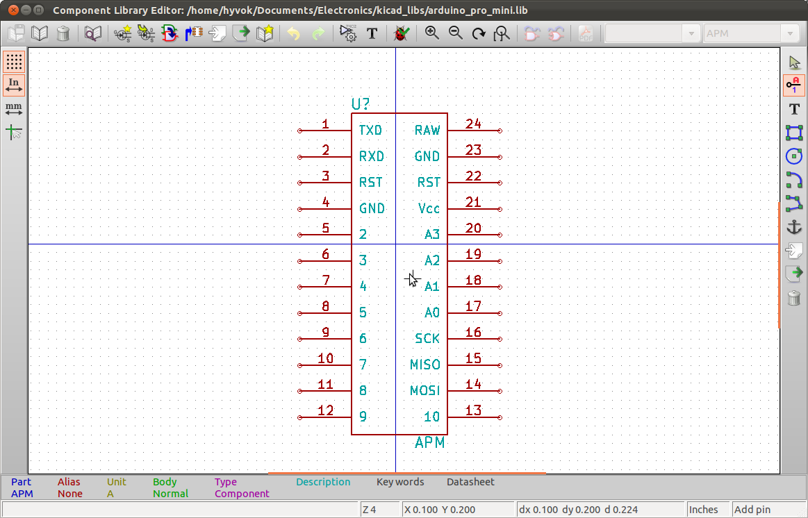
- First you have to create a library including all the components you will need for your design.This allow to add new components to a basic library by designing pin layout for a new used IC.
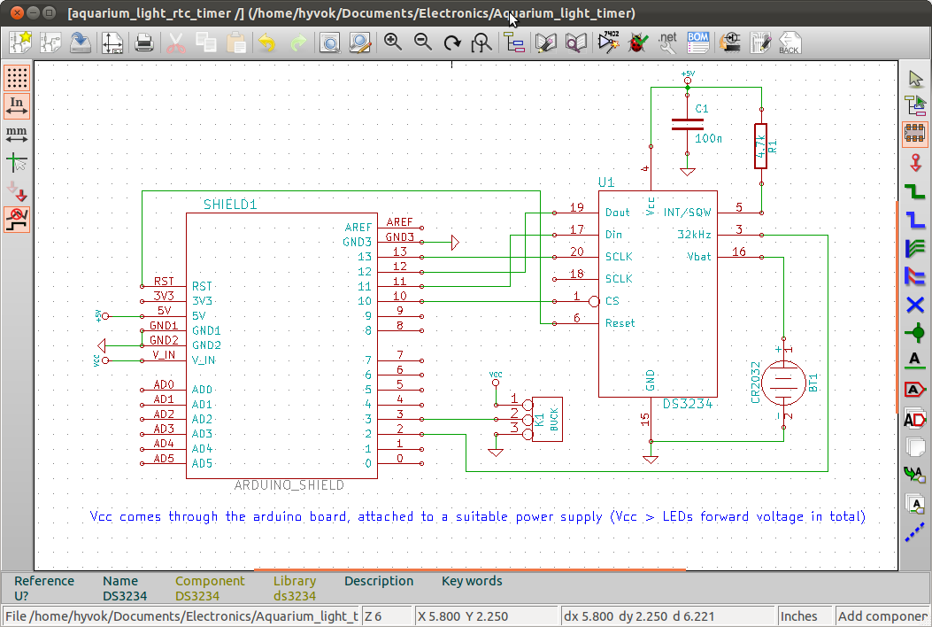
- Then you have to create a Schematic, which is the Conceptual Drawing of your electronic design. It's how components are connected together.
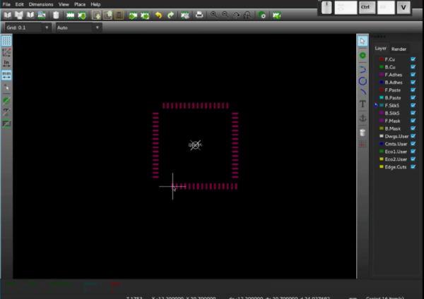
- After this you will have to make a link between components and footprints. Footprints are the layouts of pads, holes, and silkscreen drawings that are actually manufactured into the PCB, corresponding to each component.
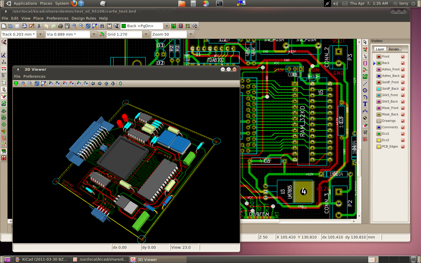
- Lastly, the PCB Design by itself. Based upon your components list and associated footprints , you can create the PCB by placing footprints at the right place and make routing between them (which is connecting components footprints by making copper paths). You can also use the famous 3D viewer to see a simulation of the result.
Once your PCB Design is finished, you can export it to Gerber Files (Vectorized layers) and send it to your favorite PCB maker.
4. Video Tutorials
5. Going Further
6.Tips
Issues with default libraries
Symbols
While the libraries are all right for some purposes, there's an issue with many of the symbols for chips. Often these symbols have hidden power pins labeled VDD and GND, or similar. KiCAD automatically connects these together, which is bad if you want them connected to a net named something else, and even worse if there is a net with one of these names which you DON'T want connected to these pins. In addition, the naming conventions on chip pins isn't consistent, and often the chip bodies are needlessly large. Therefore, it is recommended to consider copying and editing a built-in symbol.
Footprints
Many of the footprints are just fine, though some are missing 3D models. However, some common footprints, like standard types for TO-92 transistors, are missing–you will have to create them.