Table of Contents
MIDIbox 2069
The IC NJM2069
First some words about the chip.
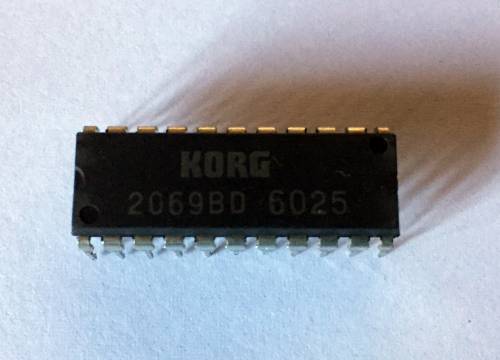
Some of you already know it. It's present in some KORG products from the 80s, in Analog Hybrid Synths like the DW and EX series, DW-6000, DW-8000, and the Poly800…

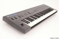
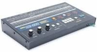
You can find it too in Some samplers of the same brand, in the DSS-1 for example.
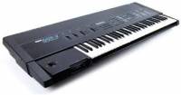

The NJM2069 is Music Voicing System, like SSM brand used to say.
Supply is a dual rail +/-5V.
Very close to the SSM2045, same functions but not the same tech. It's an OTA based LPF but it's not only a filter.
It is composed of 4 VCA and 1 VCF Low Pass 4 Poles.
2 VCA are fixed on the VCF inputs named SIG1 and SIG2. 1 is internally used for the Resonance. The last VCA if fully independent.
The VCF part has 3 Inputs:
- Signal 1 In with VCA
- Signal 2 In with VCA
- VCF Signal In direct VCF Input
2 Outputs:
- 2P Out VCF -12dB/Oct Output
- 4P Out VCF -24dB/Oct Output
and 5 CV Inputs:
- SIG1 Level
- SIG2 Level
- Freq Log
- Freq Lin
- Resonance
The Independent VCA Has is own input/output and 2 CV inputs.
First is linear CV.
The other is labelled Log in some version and seems to be a bias on another and is finally not usable, i think.
Here the function diagram and pinout.
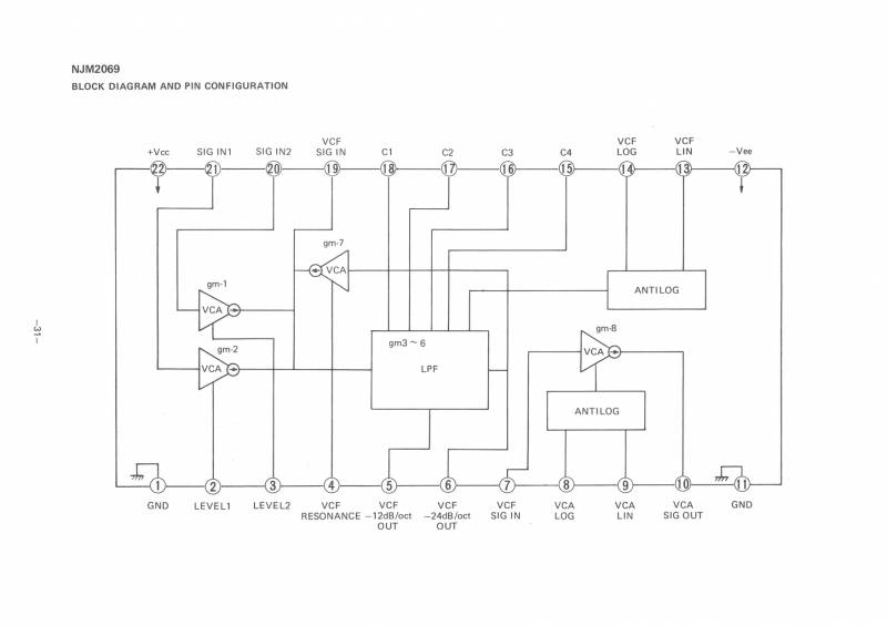
I didn't find too much documentation, no datasheet. And some written information on the internet are wrong.
For example i read somewhere that the chip is not able to self oscillate! It's wrong! Mine on a bread board do it very well ;)
Not too much data then i used the service manual of the Poly-800, DW-8000 and DSS-1 to prototype my board. And after some testing, analyze… Finally design a first PCB version.
DDS-1 Service Manual
DW-8000 Service Manual
Poly-800 Service Manual
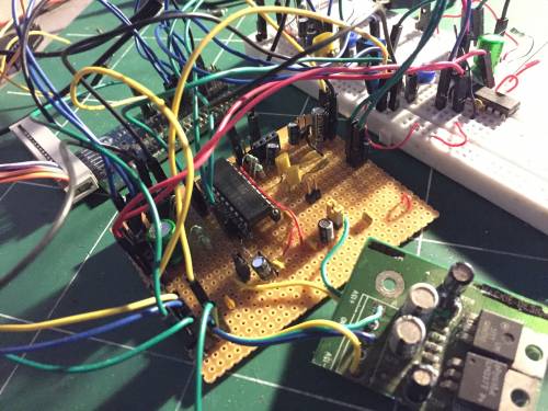
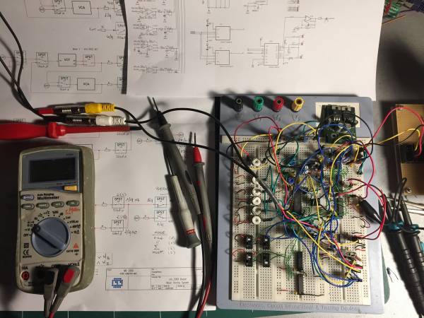
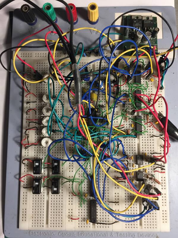
Now let's prototype it!
I used Poly-800 Service Manual page 6:
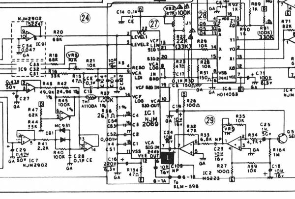
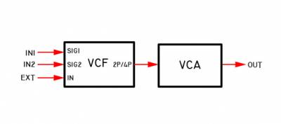
In the Poly and EX-800 the 2069 is in PRE configuration.
It means the VCA is before the VCF. The VCF has 3 Voltage controlled inputs, SIG1, SIG2 and VCF In.
Two VCO on SIG1 and SIG2 and a noise circuit is applied to the VCA In.
The VCF 4 Poles output is the Output of the filter stage.

The DW-8000 Service Manual page 22:
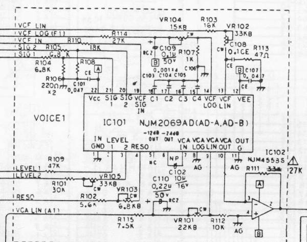
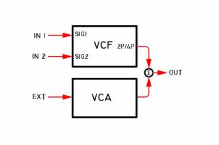
The DW-8000 is in POST config.
The VCA is after the VCF Two VCO come to SIG1 and SIG2.
The Noise Circuit is directly applied to VCF In.
The VCA Input connected to the VCF 4 poles output.
The VCA Output is the output of the filter stage.

The DSS-1 Service Manual page 18:
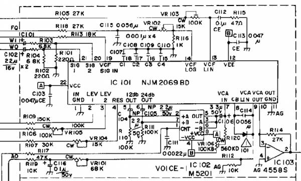
The DSS-1 is in POST config too.
The only difference is the 2 switching Op Amp added between the VCF Ouputs 2P/4P and the VCA In.

Specifications
- Digital and Analog control for all CV, both at the same time.
- Configuration modes are controllable.
- A controllable Bypass.
- Power supply is +/-12V.
- Can be use in a desktop synth or in a Modular system.
Precious information found about the 2069 once prototyped
The Absolute Rating Voltage is +/-5V, tried and fried ;)
CV inputs are in a 0 to 5V range.
All audio inputs are bipolar and support OverVoltage. A good hard clipping.
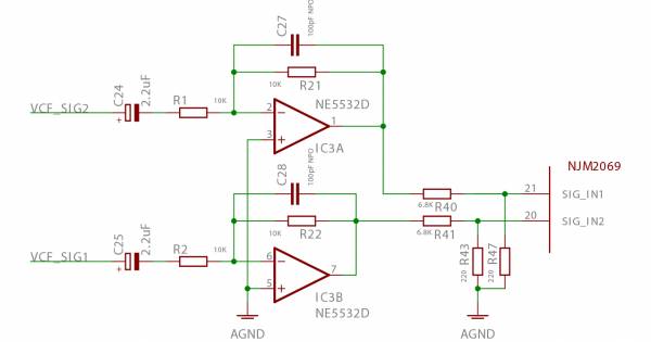
The SIG1 and SIG2 has inverted signal audio inputs.
It seems all VCA cells invert the signal, then same thing for the VCA part.
→ It will need some OP AMP, this is sure now…
LOG CV Input for cut-off Frequency is inverted input.
Lowest frequency is at 5V, Highest at 0V.
This CV needs to be inverted too.
LOG CV Input of the VCA seems unusable.
I've got only some NJM2069BD for spare then I used the D version present in my EX-800 to test Log CV of the VCA in the 2 versions, and it appears to be definitively not usable for both!
Maybe some other version (AD, DA…) of the chip release this function. I don't know.
→ But I respected and reproduced the two different existing circuit. This pin is to ground in DW-8000(AD)/EX-800(D) and acts as a kind of bias(?) in a DSS-1(BD).
Choices made during prototyping
- 2P/4P Switch, SPDT function added to the VCF outputs to switch between -12dB and -24dB… Of course.
- SPDT for ByPass Switch… Of course too!.
- DC Offset, Polarized caps to all audio inputs of the module, SIG1, SIG2, EXT(named like that to be clear) and 1 polarized cap on the output.
I checked, with some low offset Op Amps like NE5532 or NJM4580, this is enough to maintain offset and stability in all the circuit. Then no need of big and expensive bipolar caps between stages in circuit.
- Config Modes, remember, I want the switching between the configuration modes digitally controllable. (MIDI, Recall…You know why ;) I try all the valid configurations, and finally choose the 4 most interesting.
For this purpose I use 3x DG413 Analog Switch on the breadboard.
I reduced it to 1x DG333 and 1x DG413 on PCB.
All Audio purpose active components like OpAmps and Analog Switches are connected to +/-12V. We wants 2069 distortion only!
The 2069 is supplied by +/-5V, then it will be the first to saturate.
This is the block diagram of the switching circuit

Here the circuit is in default state.
The 2P/4P switch has its own line control.
The two Bypass SPST form a SPDT Switch and have their own control line too.
All others 5 switches are for Mode purpose.
5 is too much lines, remember I've got only 4 modes then I may reduce it to 2bits, 2 coding lines.
I inserted the Switches in the circuit to get this truth table:

As you can see E=B and D=C then it's reduced to 3 lines.
Now I add my 2 required inputs lines, ModeA and ModeB
We can extract that:
 It's ok, I need 1x OR gate and 1x AND gate, on PCB I use 2 small 74HC1G32 and 74HC1G08.
And finally I obtain to control everything with 4 lines:
- 1 logic line for Bypassing, Active at High.
- 1 logic line for 2P/4P switching, 4P at Low, 2P at High.
- 2 logic lines to code the 4 Configuration Modes.
Obviously you're not obliged to use this switching circuit. All I/O are individually accessible on pin header.
You can use it to access I/O or to set it in the static configuration of your choice.
- About the CV inputs of the chip: I chose to use some 0 to 5V RRIO OpAmp, for precision, voltage limiting and as DAC/CV Summing(Inverter) function.

