mios_pin_list
MIOS Pin List
This list gives you an oversight over the pin usage of MIOS.
| Name | Class | Core Port:Pin | PIC Pin # | Direction | Additional Information |
|---|---|---|---|---|---|
| RA0 | A | J5:A0 | 2 | Input | analog pin |
| RA1 | A | J5:A1 | 3 | Input | analog pin |
| RA2 | A | J5:A2 | 4 | Input | analog pin |
| RA3 | A | J5:A3 | 5 | Input | analog pin |
| RA5 | A | J5:A4 | 7 | Input | analog pin |
| RE0 | A | J5:A5 | 8 | Input | analog pin |
| RE1 | A | J5:A6 | 9 | Input | analog pin |
| RE2 | A | J5:A7 | 10 | Input | analog pin |
| RA4 | K | J4:SD | 6 | Input / Output | IIC data pin SD, external 1k pull-up, can be used by an application for other purposes so long MIOS_IIC_* won't be called |
| RC0 | B | J6:RC / J7:RC | 15 | Output | used to address the AIN multiplexers or the MF module. In both cases driven by an interrupt service routine. |
| RC1 | B | J6:SC / J7:SC | 16 | Output | used to address the AIN multiplexers or the MF module. In both cases driven by an interrupt service routine. |
| RC2 | D | J7:SO | 18 | Output | used as serial output to the MF module, driven by an interrupt service routine. |
| RC3 | C | J6:SI / J10:PWM | 17 | Output | used to address the AIN multiplexers, driven by an interrupt service routine / SID PWM. This pin is stuffed with an external 10k pull-up which could be useful for an application which uses this pin as input |
| RD0 | E | J8:SO | 19 | Output | serial output to the DOUT chain, driven by an interrupt service routine if MIOS_SRIO active |
| RD1 | E | J9:SI | 20 | Input | serial input to the DIN chain, used by an interrupt service routine if MIOS_SRIO active |
| RD2 | F | J8:RC / J9:RC | 21 | Output | serial latch output, used by an interrupt service routine if MIOS_SRIO active |
| RD3 | F | J8:SC / J9:SC / J10:SC | 22 | Output | serial clock output, used by an interrupt service routine if MIOS_SRIO active / SID SC |
| RC4 | G | J10:RC | 23 | Output | SID RC / free for applications without restrictions if second CLCD not used |
| RC5 | G | J10:SO | 24 | Output | SID SO / free for applications without restrictions |
| RD4 | E | J14 | 27 | Output | touch sensor strobe signal, used by an interrupt service routine if MIOS_SRIO active and TS_Sensitivity > 0 |
| RD5 | H | J4:SC / J10:MD / J15:RS | 28 | Output | clock output to IIC / SID MD / address signal to LCD |
| RD6 | H | J10:MU / J15:RW | 29 | Output | SID MU / RW signal to LCD |
| RD7 | I | J15:E | 30 | Output | enable signal to LCD (exclusive!) |
| RB0 | J | J15:D0 | 33 | Input / Output | LCD data line #0 |
| RB1 | J | J15:D1 | 34 | Input / Output | LCD data line #1 |
| RB2 | J | J15:D2 | 35 | Input / Output | LCD data line #2 / CAN Tx |
| RB3 | J | J15:D3 | 36 | Input / Output | LCD data line #3 / CAN Rx |
| RB4 | J | J15:D4 | 37 | Input / Output | LCD data line #4 |
| RB5 | J | J15:D5 | 38 | Input / Output | LCD data line #5 |
| RB6 | J | J15:D6 | 39 | Input / Output | LCD data line #6 |
| RB7 | J | J15:D7 | 40 | Input / Output | LCD data line #7 |
The pins are divided into following classes:
- Class A: analog inputs, which can be optionally used as digital inputs or outputs like demonstrated in the j5_dout and j5_din example if the MIOS_AIN and MIOS_MF driver are not used
- Class B: digital pin which is free for applications if neither the MIOS_AIN multiplex driver, nor the MIOS_MF driver is active Also free if MIOS_AIN doesn't run in mux mode
- Class C: digital pin which is free for applications if the MIOS_AIN multiplex driver isn't active
- Class D: digital pin which is free for applications if the MIOS_MF driver isn't active
- Class E: digital pin which is free for an application if the MIOS_SRIO driver isn't active. Can also be shared with other devices if the application accesses the pin from an interrupt service routine or if it disables all interrupts for a short time (< 300 uS!). Touchsensor Pin.
- Class F: digital pin which is free for an application if the MIOS_SRIO driver isn't active.
- Class G: free pin which can be used by the application without any restrictions
- Class H: digital pin which can be shared with other modules (LCD/IIC/…) Shouldn't be used from an interrupt service routine
- Class I: digital pin, exclusive for LCD
- Class J: digital IO pin, can be shared with the LCD data lines as IO pins so long J15:E is low (means: MIOS doesn't execute a MIOS_LCD function) Shouldn't be used from an interrupt service routine
- Class K: see description
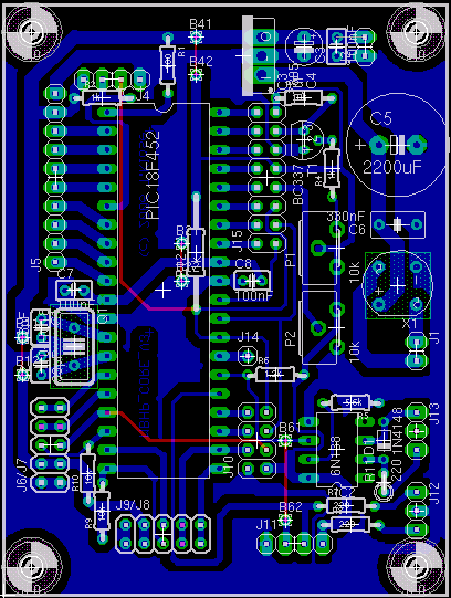
See also the schematic of the MBHP_CORE module as reference, or this PCB layout:
This table is based on the original from mios_pin_list.txt
mios_pin_list.txt · Last modified: 2011/11/29 17:01 by smashtv