Table of Contents
PAD_4*4 module
A neat way to couple WS2812B programmable LEDs (pLEDs) with a silicone button pad (e.g. Sparkfun)
Schematic
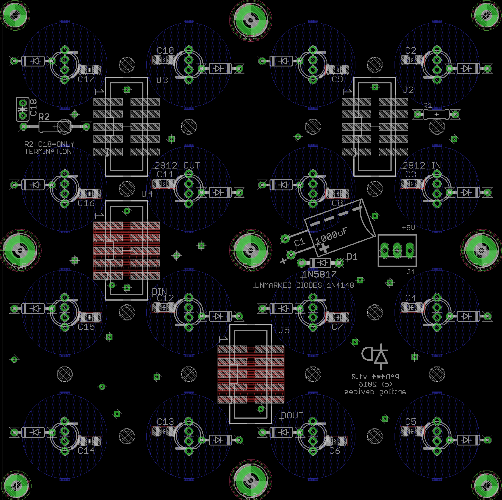
Rear view
Power input is +5V via a 3-pin 100mil connector (or Molex) and a Schottky diode. The value of electrolytic capacitor C1 is not critical.
The pLED chain enters via J2:pin 6 and resistor R1. The resistor should be replaced with a wire link for each additional module (i.e. only the first in the chain gets a resistor, the remainder stuffed with wire links). The serial chain then follows a snake pattern to J3, where additional pLED modules may be connected. The RC (R2, C18) end termination shouldn't be necessary, but can be trialled should problems with signal reflection arise.
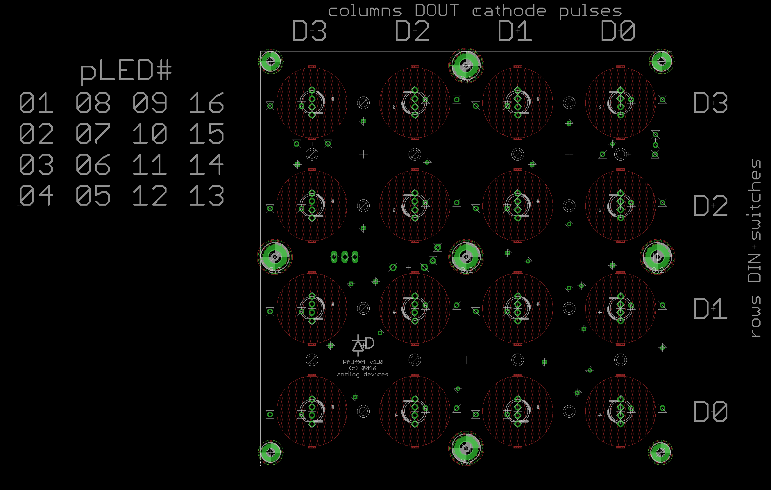
Front view
Switches are connected in a 4*4 matrix with the given mapping. D0 refers to pin 10 of the IDC header (i.e. top right) for both DIN and DOUT.
BOM v1.1
| Type | Qty | Value | Package | Parts | Notes |
|---|---|---|---|---|---|
| resistors | |||||
| 1 | 220-470R | 0204/7 | R1 | replace with wire link for each additional module | |
| capacitors | |||||
| 16 | 100n | 1206 | C2-17 | ||
| 1 | 100-1000u | electrolytic 3,5-6 | C1 | ||
| diodes | |||||
| 1 | 1N5187 | DO41-7.6 | D1 | ||
| 16 | 1N4148 | DO41-7.6 | remaining axial diodes | ||
| 16 | WS2812B | 5mm | programmable LEDs | ||
| headers | |||||
| 4 | 2*5 (shrouded) SMT | J2-5 | can use DIL 100mil breakaway header strips | ||
| 1 | 1X03_SMALL | J1 | can use Molex 22-23-2031 | ||
| switches | |||||
| 1 | Sparkfun 4×4 pad | ||||
| misc | |||||
| 1 | acrylic bezel |
Versions
v1.1: current release. Some traces moved around, grounding error fixed. J1 power header changed to offset pads so an SMT pinheader may be soldered if desired.
v1.0: errata: J4 and J5 have no connection to ground. J1-3 do carry ground, so it isn't a problem if the DIN/DOUT modules share the same power rail.
Assembly
To keep the button pad flat, it's best to solder all components on the rear of the board i.e. opposite the pads. The contacts are exposed ENIG, so try not to damage the surface by scratching or splashing solder/flux on them.
Start by tinning one pad (preferably not the pad joined to the ground plane with thermals) of each 1206 capacitor, making a “tack” joint, aligning the part and cleaning up if needed.
The best way to fix the 1N4148 diodes is to place the parts then solder from the same side just the anode lead that intersects the pLED silkscreen. (The length of this lead isn't important as the LED will not be flush on the top face. Don't short out any pins though!) Turn the board around and clip the cathode lead as close to the board as possible. You can even pull the loose lead out slightly as long as you can still make a solid joint. On the rear of the board, solder the cathode with as little solder as possible. The aim is to leave no solder bump on the frontside. Try to give equal care to the other through hole components (R1, C1, D1, J1).
Check that the pinout of your pLEDs matches with the board i.e. serial in on the rounded side, serial out on the flattened side. Also test the height relative to the silicone button pad; it's not necessary to push the leads in the whole way (and you might damage your LED).
If using shrouded headers, ensure the notch points out on the same side as the pin 1 designator.
Interconnections
- J2 normally connects to Core J4B (I2C)
- J3 carries the WS2812B chain for additional modules
- J4 connects to a DIN header
- J5 connects to a DOUT header
License
Currently the design is © 2016 antilog devices with all rights reserved; all documentation is CC BY-NC-SA 3.0.