Table of Contents
SCS OLED module
Combination of 0.96“ SSD1306 OLEDs and switches for an SCS
Schematic
Refer to the SCS schematic or below for J1/button and encoder pinning and the Core module (J15) for J5/OLEDs.
BOM v1.0
| Type | Part | Value |
|---|---|---|
| Caps | C25 | DNF |
| C26 | DNF | |
| C29 | 10uF polarised | |
| Encoder | EN1 | 12mm |
| EN2 | 12mm | |
| Header | J1 | PINHD-2X54WALL |
| J2 | +5V | |
| J5 | PINHD-2X54WALL | |
| OLEDs | LCD1 | 0.96_OLED |
| LCD2 | 0.96_OLED | |
| LCD3 | 0.96_OLED | |
| LCD4 | 0.96_OLED | |
| Resistors | R3 | DNF |
| R4 | DNF | |
| R7 | DNF | |
| R9 | 2k2 | |
| Switches | S1(A) | DT6 or 6mm |
| S2(A) | DT6 or 6mm | |
| S3(A) | DT6 or 6mm | |
| S4(A) | DT6 or 6mm | |
| S5(A) | DT6 or 6mm | |
| S6(A) | DT6 or 6mm |
Versions
v1.0: first release
Assembly
Decide on the configuration to be used. Any combination of switches, encoders or OLEDs is possible if they fit.
Only one encoder is wired to the J1 header. If you want to use the EN2 position, wire the legs to the empty EN1 solder points.
R9 and C29 form the power-on reset for OLEDs. R7 should not be installed. R3/C25/R4/C26 form a termination shunt for OLED data lines. They shouldn't be required.
The switches accommodate either DT6 or 6mm switches (obviously only one type!). For DT6 switches, ensure the flat side is aligned with the PCB silkscreen.
J2 can supply power if needed.
Interconnections
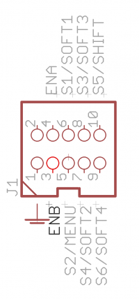
J1 is the SCS header, connecting to J10A
J2 can provide power as indicated; it is also connected on J5.
J5 connects to J15 on the Core (or equivalent)
Dimensions

License
Currently the design is © 2016 antilog devices with all rights reserved; all documentation is CC BY-NC-SA 3.0.