Table of Contents

Summary
The MBHP_Genesis module provides all the hardware necessary to support one of each YM2612/YM3438 (OPN2) and SN76489/94/96 (PSG) sound chips and interface them to a microcontroller (including one of the MIDIbox core modules). In addition, the circuit and board are designed so that up to four MBHP_Genesis modules may be stacked on top of each other to run up to four sets of sound chips, with simple pin/socket headers connecting the boards and no additional wiring needed.
Features:
- High-speed parallel interface to both sound chips, optimized for CORE_STM32F4 ports J10A and J10B, but compatible with most MCUs; requires no other signal connections to the core
- SN76489/94/96 has data latch with automatic deselection, so the MCU can write to it and then immediately use the bus for other things, rather than having to leave the data on the bus until the chip asserted READY
- YM2612/3438 Test and /IRQ pins, and SN76489/94/96 Ready pin, are readable from the core via the parallel interface
- YM2612/3438 Test pin has selectable direction (with protection), and both Test and /IC pins can be written to from the core via the parallel interface
- Analog buffering, filtering, and mixing onboard, all from same +5V power supply (no bipolar +/-12V supply), with OPN2/PSG mixer/pan/volume potentiometer connections
- Filter cutoff frequency selectable between two options (unfiltered or Mega Drive Model 1 mode), separately selectable for OPN2 channels and PSG channel; selection controlled via parallel interface
- SN76494/96 Audio In pin fully supported, with protection
- Separate oscillators for each sound chip; supports 8-DIP or 5x7mm SMT packages
- All parts DIP/through hole (no SMT) (except for optional SMT oscillator)
- Smallest footprint (cheapest board) possible
- Many components may be left unstuffed if certain features not desired
- Available now for only $5 on the MIDIbox Shop!
Disadvantages:
- Very dense layout
- Larger board than it would be if all the glue logic was removed, and more wires were used to interface to the core (though certain aspects if 2 or 4 boards were used, e.g. reading Ready signals from the PSGs, would require multiple wires or additional logic)
- Parallel interface is +5V, which may cause issues with CORE_STM32F4 (3.0V) or other MCUs at 3.3V. If using only one MBHP_Genesis module, it might work (pending testing) assuming the core tolerates 5V inputs (as CORE_STM32F4 does). However, for two or more boards, due to fanout, an external level shifter circuit will be required. See MBHP_Genesis_LS.
MBHP_Genesis Module Hardware
Links
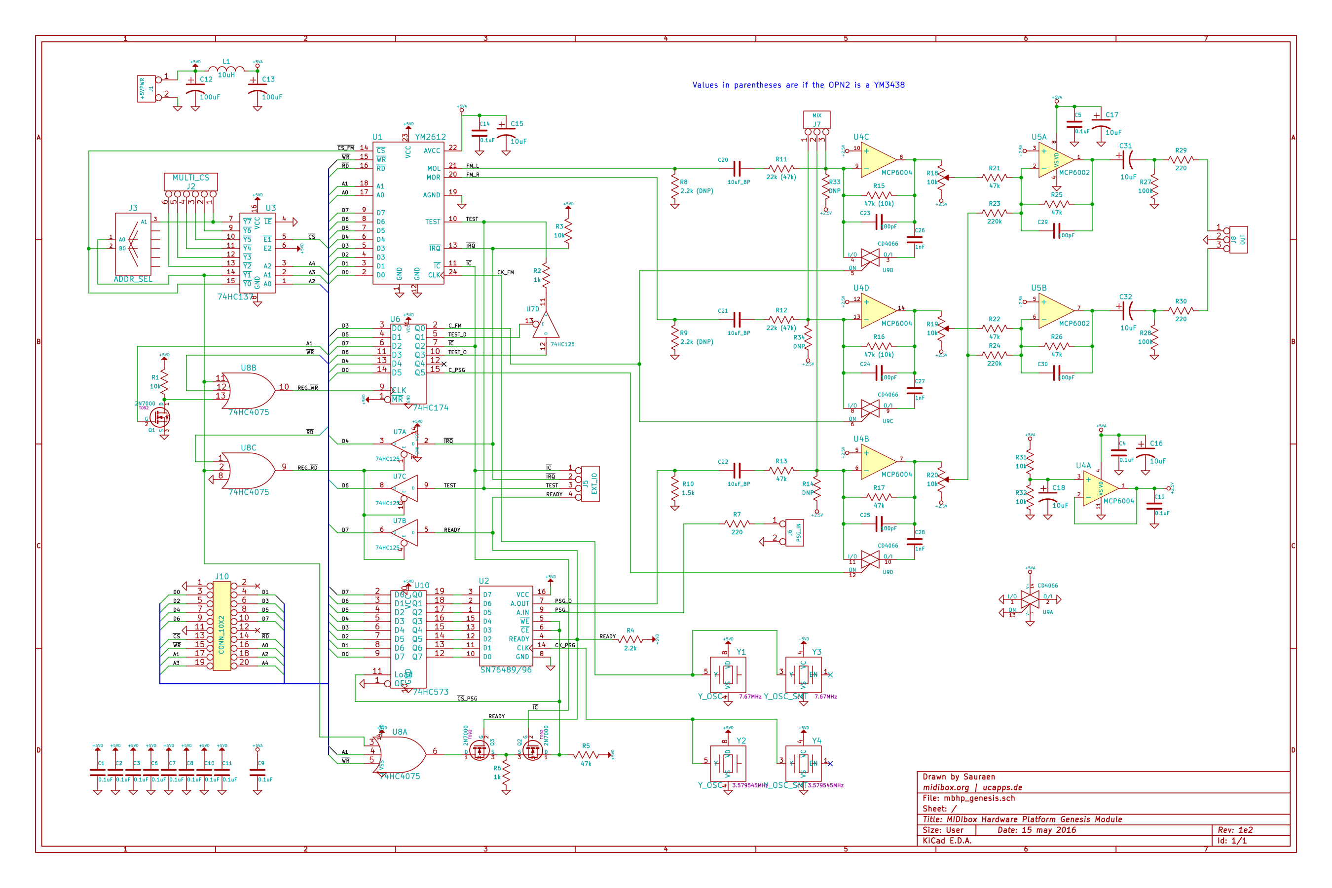
- Schematic (rev. 1e2, for production version boards rev. 1e) (full size version try here)
- MIDIbox Gallery for MIDIbox Quad Genesis, containing many pictures of the MBHP_Genesis module
Pinout
Most of this is really easy to read off the schematic, but here you go anyway.
J1: +5VPWR
+5V power input to the module.
| Pin | Label | Function |
|---|---|---|
| 1 | +5VD | 5V supply to board. The “D” stands for “digital”, in comparison to the +5VA net which is the supply for all analog circuitry. |
| 2 | GND | Ground. Common to analog and digital. Not connected to the mounting holes. |
J2: MULTI_CS
Chip-select lines generated by the decoder on the first board, for the sound chips on the other three boards.
| Pin | Label | Function |
|---|---|---|
| 1 | – | /CS for PSG and onboard registers on Board 4 |
| 2 | – | /CS for YM2612 on Board 4 |
| 3 | – | /CS for PSG and onboard registers on Board 3 |
| 4 | – | /CS for YM2612 on Board 3 |
| 5 | – | /CS for PSG and onboard registers on Board 2 |
| 6 | – | /CS for YM2612 on Board 2 |
J3: ADDR_SEL
This is a fun one. This connector allows you to specify which board each board is, by selecting which pair of /CS lines from the decoder are used on each board. It shares pads with the decoder, U3. Here's how to connect it:
- On board 1, stuff U3 and its bypass capacitor C3, but don't connect anything in J3.
- On board 2, don't stuff U3 or C3, but connect two wires on the top of the board, one from U3:13 to J3:2, and one from U3:12 to J3:1. They should follow the first two angled lines on the footprint for J3 under U3.
- On board 3, same thing but connect U3:11 to J3:2 and U3:10 to J3:1. These two wires should follow the second set of lines on the board, the non-angled ones.
- On board 4, same thing but connect U3:9 to J3:2 and J3:3 to J3:1. These two wires should follow the last pair of lines on the board, angled in the opposite direction.
The overall effect is that the eight signals from the decoder are distributed in pairs to each of the boards. J3:2 and J3:1 are connected to U3:15 and U3:14, so on the first board the decoder drives the two /CS lines directly.
J5: EXT_IO
For those who prefer to have separate wires from the module to the core for the additional signals to/from the sound chips, rather than using the parallel interface to read/write them, this header brings them out.
| Pin | Label | Function |
|---|---|---|
| 1 | /IC | YM2612/3438 reset signal. Don't drive this pin externally if U6 is stuffed! |
| 2 | /IRQ | YM2612/3438 interrupt request signal. Goes low when one of the OPN2 timers overflows if configured approrpriately. |
| 3 | TEST | YM2612/3438 Test signal. See Notes about the YM2612's Test pin. |
| 4 | Ready | SN76489/94/96 Ready signal. Also called /BUSY. Goes high when the chip is ready to receive new data. |
J6: PSG_IN
Audio input to the PSG's analog audio input pin, if the PSG used is a SN76494 or SN76496.
| Pin | Label | Function |
|---|---|---|
| 1 | – | Audio input. See the PSG's datasheet, and choose the value of R7 accordingly. |
| 2 | GND | Ground. |
J7: MIX
These are the three nodes where the audio signals from the different boards' YM2612 and PSG channels are mixed. The three pins correspond to the summing node of an inverting amplifier with first-order low-pass filter.
| Pin | Label | Function |
|---|---|---|
| 1 | – | OPN2 Right channel summing node |
| 2 | – | PSG mono summing node |
| 3 | – | OPN2 Left channel summing node |
This means that if you're using two or more boards, stuff everything up to J7 on all boards, and connect each pin of J7 across all boards. Then, only stuff the parts downstream of J7 on one of the boards, and take the audio output from J8 on that board. (This is assuming you want everything mixed into one stereo pair.)
R18, R19, R20
These are three-pin headers to connect potentiometers to adjust the relative volume (and panning if desired) of the OPN2 and PSG. As is obvious from the schematic, R18 is for OPN2 Left, R19 is for OPN2 Right, and R20 is for PSG. The potentiometer is 10k nominal (will work fine with 5k or 2k), audio type (A) preferred but not required. It is intended that a dual-gang potentiometer would be used to adjust the OPN2 levels together, and a separate single one for the PSG. If panning is desired, after the level potentiometers, connect a 20k or 50k potentiometer between the Left output and Right output (R18:2 and R19:2) with its wiper connected to +2.5V (R18:1).
J8: OUT
Analog audio output from all the modules together. Low-impedance output, referenced to ground.
| Pin | Label | Function |
|---|---|---|
| 1 | – | Left channel output |
| 2 | GND | Ground |
| 3 | – | Right channel output |
J10: DATA
Parallel address and data busses between MCU and module. Pins 1 through 10 connect to J11A on the core and pins 11 through 20 connect to J11B.
| Pin | Label | Function |
|---|---|---|
| 1 | GND | Ground |
| 2 | – | No connection (+3.3V or +3V from the core, not used on module) |
| 3 | D0 | Least-significant data line |
| 4 | D1 | Data line |
| 5 | D2 | Data line |
| 6 | D3 | Data line |
| 7 | D4 | Data line |
| 8 | D5 | Data line |
| 9 | D6 | Data line |
| 10 | D7 | Most-significant data line |
| 11 | GND | Ground |
| 12 | – | No connection (+3.3V or +3V from the core, not used on module) |
| 13 | /CS | Chip Select for entire module, active-low |
| 14 | /RD | Read strobe for entire module, active-low |
| 15 | /WR | Write strobe for entire module, active-low |
| 16 | A0 | Least-significant address line, selects OPN2 address or data |
| 17 | A1 | Address line, selects OPN2 register set and PSG/register on write |
| 18 | A2 | Address line, selects OPN2 or PSG/registers |
| 19 | A3 | Address line, selects board index LSB |
| 20 | A4 | Most-significant address line, selects board index MSB |
Parts list
Mouser part numbers are included for convenience, all parts (besides the two sound chips) are standard and should be available at any electronics site (e.g. Reichelt). Parts labeled “buy in bulk” should already be in your electronics inventory; they are of course available at Mouser and elsewhere if you don't have any, but you should probably buy many more than are necessary for this project (e.g. resistors in sets of 100 or 200 of the same value from eBay).
| Qty | Ref. Deg. | Part Name | Mouser Part Number | Description / Notes |
|---|---|---|---|---|
| 1 | U1 | YM2612 or YM3438 | N/A | OPN2 chip, available on eBay for about $5 or less |
| 1 | U2 | SN76489 or SN76494 or SN76496 | N/A | PSG chip, available on eBay for about $2 or less |
| 1 | U3 | 74HC137 | 595-CD74HC137E | 3-to-8 decoder with enable, for selecting board and sound chip |
| 1 | U4 | MCP6004 | 579-MCP6004-I/P | Rail-to-rail 5V quad op-amp with appropriate characteristics |
| 1 | U5 | MCP6002 | 579-MCP6002-I/P | Rail-to-rail 5V dual op-amp with appropriate characteristics |
| 1 | U6 | 74HC174 | 595-SN74HC174N | Hex flip-flop for board data input bits; CD40174 works but 74HC174 preferred due to stronger drive capability |
| 1 | U7 | 74HC125 | 595-SN74HC125N | Quad tristate buffer for board data output bits |
| 1 | U8 | 74HC4075 | 595-CD74HC4075E | Triple 3-input OR for glue logic; CD4075 (barely) works but voltage levels are not pretty in Q2-Q3-U2 circuit, 74HC4075 much preferred |
| 1 | U9 | CD4066 | 595-CD4066BE | Quad transmission gate, for digitally-switchable filter capacitors |
| 1 | U10 | 74HC573 | 595-SN74HC573AN | Octal transparent latch, for storing data to PSG so bus may be used for other transactions |
| 1 | [U1] | 24-pin 0.6“ DIP socket | 517-4824-6000-CP | Socket for OPN2 |
| 3 | [U2], [U3], [U6] | 16-pin 0.3” DIP socket | 571-1-2199298-4 | Sockets for three 16-pin DIP ICs |
| 4 | [U4], [U7], [U8], [U9] | 14-pin 0.3“ DIP socket | 571-1-2199298-3 | Sockets for four 14-pin DIP ICs |
| 1 | [U5] | 8-pin 0.3” DIP socket | 571-1-2199298-2 | Socket for MCP6002 |
| 1 | [U10] | 20-pin 0.3“ DIP socket | 571-1-2199298-6 | Socket for 74HC573 |
| 1 | Y1 or Y3 | 7.67 MHz (or 8 MHz) oscillator | 774-MXO45HS-3C-8.0 | Oscillator (either half-size/8-DIP or 5x7mm SMD) at desired OPN2 frequency. MIDIbox Genesis firmware will correct frequencies to match original VGM pitch, but if this is your own project, careful selection and/or custom clock circuitry may be necessary. |
| 1 | Y2 or Y4 | 3.58 MHz (or 4 MHz) oscillator | 520-TCH357-X | Oscillator (either half-size/8-DIP or 5x7mm SMD) at desired PSG frequency. MIDIbox Genesis firmware will correct frequencies to match original VGM pitch. |
| 3 | Q1, Q2, Q3 | 2N7000 or BS170 | 821-TSM2N7000KC821-T or 512-BS170 | Any small-signal N-channel MOSFET with the gate as the center pin; the board silkscreen is for 2N7000, if you use BS170 (as I did) mount them backwards to match the source and drain pins. |
| - | J1, J2, J7, J10 | 0.1” stackable pin socket/headers | 782-A000086 | Pin sockets with long pins (from Arduino shields), for stacking the boards together. Buy in bulk and combine them for the appropriate sizes. Use a regular pin header for the lowest board in the stack; have each header mounted with the socket below the board and the pins sticking out the top. See this photo of the stack. |
| - | J5, J6, J8 | 0.1“ pin headers | Buy in bulk | Headers; J5 and J6 are individual on each board if used, and J8 is only on the final board. |
| 1 | L1 | 10 uH inductor | 434-SMCCN-100K-02 | For LC filter for analog power rail |
| 2 | C12, C13 | 100 uF electrolytic | Buy in bulk | Power rail filter caps |
| 4 | C15, C16, C17, C18, C31, C32 | 10 uF electrolytic | Buy in bulk | Analog power rail filter caps |
| 3 | C20, C21, C22 | 10 uF bipolar electrolytic | 647-UVP1C100MDD | Audio high-pass filter caps |
| 13 | C1:C11, C14, C19 | 0.1 uF ceramic / monolithic / film | Buy in bulk | IC power rail filter caps |
| 3 | C23, C24, C25 | 180 pF ceramic / etc. | Buy in bulk (maybe) | Stability filter caps (above hearing range) |
| 3 | C26, C27, C28 | 1 nF ceramic / etc. | Buy in bulk | Filter caps for Mega Drive / Genesis - style filter |
| 2 | C29, C30 | 100 pF ceramic / etc. | Buy in bulk | Stability filter caps (above hearing range) |
| 2 | R1, R3 | 10k ohm 5% or better 0.25W carbon-film or metal-film axial through-hole vertically-mounted resistor | Buy in bulk | Pull-ups for digital lines |
| 2 | R2, R6 | 1k blah blah blah regular resistor | Buy in bulk | R2: protecting TEST pin from contention, R6: part of Q2-Q3-U2 latch circuit |
| 1 | R4 | 2.2k resistor | Buy in bulk | Pull-up for PSG READY line |
| 1 | R5 | 47k resistor | Part of Q2-Q3-U2 latch circuit | |
| 1 | R7 | 220 ohm resistor or DNP | Buy in bulk | Protection for SN76494/SN76496 audio input (omit for SN76489 as there is no audio input) |
| 2 | R8, R9 | 2.2k resistor or DNP | Buy in bulk | Load for YM2612 (omit for YM3438) |
| 1 | R10 | 1.5k resistor | Buy in bulk | Load for PSG |
| 2 | R11, R12 | 22k or 47k | Buy in bulk | Mixing resistors for OPN2: 22k for YM2612, 47k for YM3438 |
| 2 | R15, R16 | 47k or 10k | Buy in bulk | Mixing resistors for OPN2: 47k for YM2612, 10k for YM3438 |
| 3 | R14, R33, R34 | — | — | Do not populate |
| 7 | R13, R17, R21, R22, R25, R26 | 47k resistor | Buy in bulk | Mixing and filtering resistors |
| 1 | R18/R19 | 10k potentiometer(s) | Front panel specific | OPN2 volume control; single dual-gang 10k audio (or linear) potentiometer, to be mounted on your front panel |
| 1 | R20 | 10k potentiometer | Front panel specific | PSG volume control; regular 10k audio (or linear) potentiometer, to be mounted on your front panel |
| 2 | R23, R24 | 220k resistors | Buy in bulk | If you want a louder PSG, reduce the value |
| 2 | R27, R28 | 100k resistors | Buy in bulk | High-pass filter resistors |
| 2 | R29, R30 | 220 ohm resistors | Buy in bulk | Audio output short-circuit protection resistors |
| 2 | R31, R32 | 10k 1% resistors | Buy in bulk | For voltage divider to set the virtual ground |
Mixing resistors
Previously I had a section here about the different use cases and what values of resistors to use for R11 through R17. But since I've finished the hardware for two MIDIbox Quad Genesises, one with four YM2612s and one with four YM3438s, I think the values are pretty much final at this point. I have not tested extreme cases for clipping (e.g. all four YM3438s in DAC Override mode playing peak-to-peak samples), but my calculations based on measurements of normal audio suggest that even this won't clip (though to be honest, I'm not sure if clipping in that situation would be a bad thing).
The values I used for my quad builds are on the schematic and in the parts list. The normal values are for use with YM2612s, and the values in parentheses are the ones to use with YM3438s. All other parts which just show one value are the same on both builds.
Component stuff chart
Here is a chart of what components should be stuffed on each build configuration I could think of. In most cases, several of these build configurations will be active at the same time (e.g. in a typical four-board setup, the top board is A, B or C, D, (E), F, G, H, I, M. Note that MIDIbox Quad Genesis requires F, G, H, I).
| Label | Description |
|---|---|
| A | Any board you want to include a YM2612/3438 |
| B | YM2612 only |
| C | YM3438 only |
| D | Any board you want to include a SN76489/94/96 |
| E | If a PSG is included and it is SN76494 or SN76496 and you want Audio In support |
| F | If you want to read Test, /IRQ, or Ready via parallel interface |
| G | If you want to write Test or /IC via parallel interface |
| H | If you want digitally-controllable filter capacitors via parallel interface |
| I | If you want to read/write Test, /IRQ, /IC, or Ready directly to/from each board |
| J | One board, YM2612 only, no parallel glue logic |
| K | One board, SN764** only, no parallel glue logic |
| L | One board, both chips, no parallel glue logic |
| M | Two or four boards, first board; or one board, both chips and parallel glue logic |
| N | Two or four boards, second board |
| O | Four boards, third board |
| P | Four boards, fourth board |
Here is the chart of all parts, and which configurations they should be stuffed in:
| Parts | A | B | C | D | E | F | G | H | I | J | K | L | M | N | O | P |
|---|---|---|---|---|---|---|---|---|---|---|---|---|---|---|---|---|
| U1, C1, C14, C15, Y1 or Y3, C20, C21, R11, R12 | X | |||||||||||||||
| R8, R9 | X | |||||||||||||||
| R33, R34 | X | |||||||||||||||
| U2, C2, Y2 or Y4, U10, C10, Q2, Q3, R4:6, R10, C22, R13 | X | |||||||||||||||
| J1, C12, L1, C13, C11 | X | X | ||||||||||||||
| J6, R7 | X | |||||||||||||||
| U7, C7 | X | X | ||||||||||||||
| U8, C8 | X | X | X | |||||||||||||
| U6, C6, Q1, R1 | X | |||||||||||||||
| U9, C9 | X | |||||||||||||||
| J5 | X | |||||||||||||||
| Short U3:5 to U3:15 | X | |||||||||||||||
| Short U3:5 to U3:14 | X | |||||||||||||||
| Short U8:3 to U8:6 | X | X | ||||||||||||||
| U3, C3, J2 | X | X | ||||||||||||||
| U4, C4, U5, C5, C16:19, C23:32, R15:32, J8 | X | X | X | X | ||||||||||||
| Short U3:13 to J3:2, short U3:12 to J3:1 | X | |||||||||||||||
| Short U3:11 to J3:2, short U3:10 to J3:1 | X | |||||||||||||||
| Short U3:9 to J3:2, short J3:3 to J3:1 | X | |||||||||||||||
| J10 | X | X | X | X | X | X | X |
Construction differences by sound chip type
Here's the relevant differences between the sound chips:
| PSG Chip | Nominal clock | Audio in? |
|---|---|---|
| SN76489 | 4 MHz | No |
| SN76494 | 500 kHz | Yes |
| SN76496 | 4 MHz | Yes |
| OPN2 Chip | Technology | Audio output volume | “Ladder effect” DAC error |
|---|---|---|---|
| YM2612 | NMOS | Quiet | Yes |
| YM3438 | CMOS | Loud | No |
For the PSG chips, the relevant differences are obvious: use the correct clock speed for the chip, and do or don't connect an audio input. It's much easier to find 4 MHz (or 3.58 MHz) oscillators for the '89 and '96 than a 500 kHz oscillator for the '94, so you're a bit on your own if you choose that chip.
For the OPN2 chips, the YM3438 is a complete reimplementation of the YM2612 in CMOS instead of NMOS. They also changed the output stage to get rid of some analog error in the YM2612's DAC, which produces a distinctive “ladder effect” sound in the audio output, as well as making the output about 10-20dB louder (which also produces excellent signal-to-noise performance). FM synthesis purists might be inclined to choose the YM3438; retro gaming fans will probably go with the YM2612, as this is the physical chip used in the Mega Drive / Genesis Model 1.
(Note about the next two paragraphs: the resistor values given in the parts list are the ones I used and tested for each of YM2612 and YM3438, there's no clipping or other issues. If you don't want to experiment, use those.)
The differences for this module are relatively simple. For a YM2612, the audio outputs require a known load to perform to spec–these are R8 and R9. The value of 2.2k was taken from the Mega Amp design, but some experimentation may be warranted.
For a YM3438, no load is necessary (don't stuff R8 and R9), but it's loud enough that it may clip when four are mixed together. Also you may want to reduce the volume if you have two YM3438s and two YM2612s. This is set by the relative sizes of R11, R33, and R15 on the left channel, and R12, R34, and R16 on the right.
MBHP_Genesis Module Software
Memory map
Here's the memory map for the case of four modules in parallel with all features included:
(Syntax like VHDL: -=don't care, X=forced unknown, Z=high-impedance; MN = module index [00,01,10,11])
| /CS | /RD | /WR | A4 | A3 | A2 | A1 | A0 | D7 | D6 | D5 | D4 | D3 | D2 | D1 | D0 |
|---|---|---|---|---|---|---|---|---|---|---|---|---|---|---|---|
| 1 | - | - | - | - | - | - | - | Z | Z | Z | Z | Z | Z | Z | Z |
| 0 | 1 | 1 | - | - | - | - | - | Z | Z | Z | Z | Z | Z | Z | Z |
| 0 | 0 | 1 | M | N | 0 | - | - | OPN2 Busy | X | X | X | X | X | OPN2 TmrA Oflw | OPN2 TmrB Oflw |
| 0 | 0 | 1 | M | N | 1 | - | - | PSG Ready | OPN2 Test | X | OPN2 /IRQ | X | X | X | X |
| 0 | 1 | 0 | M | N | 0 | 0 | 0 | OPN2 Address Write Part 1 | |||||||
| 0 | 1 | 0 | M | N | 0 | 1 | 0 | OPN2 Address Write Part 2 | |||||||
| 0 | 1 | 0 | M | N | 0 | - | 1 | OPN2 Data Write | |||||||
| 0 | 1 | 0 | M | N | 1 | 0 | - | PSG Address/Data Write (latched) | |||||||
| 0 | 1 | 0 | M | N | 1 | 1 | - | OPN2 /IC | OPN2 Test Data Out | OPN2 Test Data Dir | - | OPN2 Cap Select | - | - | PSG Cap Select |
| 0 | 0 | 0 | - | - | - | - | - | Illegal state, bus contention | |||||||
Bus timings
Idle
- /CS, /RD, and /WR are all 1. A4:0 and D7:0 are -.
Write cycle
- Set the data direction of D7:0 on the MCU to outputs.
- Write the write data to D7:0.
- Write A4:0.
- Write /WR to 0 (this can be done in the same operation as writing A4:0 above)
- Write /CS to 0 (this should not be the same operation as above, but ~20ns later)
- Set MCU data port pins to output mode.
- If the write is to the OPN2, wait a little over 6 OPN2 clocks. If the write is to the PSG latch or local register (OPN2 /IC, Test, Caps), wait about 50ns (propagation delay of all onboard logic).
- Set MCU data port pins to input mode.
- Write /CS to 1.
- Write /WR to 1.
- Set the data direction of D7:0 on the MCU to inputs.
For the OPN2, repeat the above for the data write.
Read cycle
- Write A4:0 to MN0– if the write was OPN2, or MN1–if the write was PSG.
- Write /RD to 0 (this can be done at the same time)
- Write /CS to 0 (not at the same time)
- Read D7:0. (If waiting for the chip to not be busy, loop here; output data to MCU is not latched, it will update in real time.)
- Write /CS to 1.
- Write /RD to 1.
Notes about the YM2612's Test pin
From reading photomicrographs of the YM2612 die and further related hacking work, it has been confirmed that this is an I/O pin, not just an output. Hence the MBHP_Genesis module contains circuitry to both read and write the pin on each YM2612 independently, as well as to select the pin direction. If the pin is mistakenly configured as an input (so the module drives it) while the YM2612 is also driving it, a protection resistor R2 allows the YM2612 to override the state of the line without damage to either device.
When appropriately configured as such via bits in the test registers discovered by Sauraen, the Test pin outputs a SYNC signal–a pulse for one of the 24 operators in the cycle. Using this pulse to know when to start and putting the OPN2 in a particular test mode, MIDIbox Quad Genesis periodically reads out the state of all 24 operators, and measures the average volume of the operator for the VU meter display on the front panel.