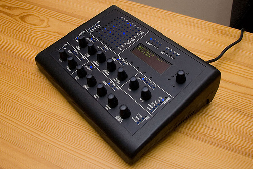
MB-6582 - MIDIbox SID Synthesizer V2
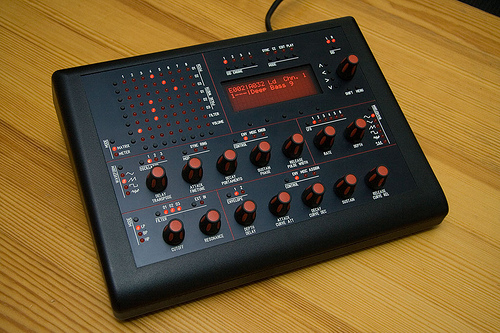
MB-6582 is a MIDIbox SID synthesizer.
If you have no idea what that is, look here:
http://www.ucapps.de/midibox_sid.html
More photos of MB-6582 during construction
http://www.flickr.com/photos/wilba/
PCBs and knobs are now available at Modular Addict.
https://modularaddict.com/manufacturer/midibox
For SID chips, PIC chips, panels, and any other parts you're having trouble sourcing, your best bet is to ask around at the forums.
To get you started on your BOM, you can use this Excel spreadsheet kindly made by dwestbury. For more info, see this forum post.
The MB-6582 project is based on the MIDIbox Hardware Platform (MBHP) and is strictly for personal non-commercial use. Everyone who has bought MB-6582 PCBs must read and agree to the following license:
The official list of MB-6582 Builders, with serial numbers
The Original MB-6582, aka. the MB-6582 Prototype (old pages)
Introduction
MB-6582 is the name of my MIDIbox SID Synthesizer V2 project.
When it was finished, I was totally surprised that it was making appearances on many blogs, but what surprised me the most was when it appeared on Hack-a-day:
“This is one of the nicest DIY builds I've seen in a while - just beautiful work.” - Will O'Brian, Hack-a-day
However, this one was the most amusing:
“Sometimes you see a DIY project and you're just like “are you fucking kidding me? This is one such, for sure. This dude's MIDIbox SID is a DIY synth the way that an Aston Martin Vanquish is a car. I mean, like, fuck. Eight (as in “the number after seven”) 6582 SID chips for four stereo (as in “mono times two”) channels of audio, a nice FPE panel, and the same number of LEDs as any random sign in Times Square.” - Chris Randall, Analog Industries
But my favourite bit of praise:
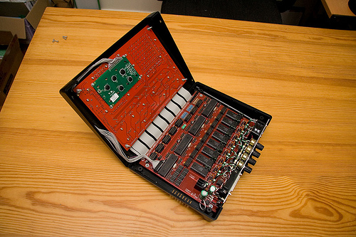
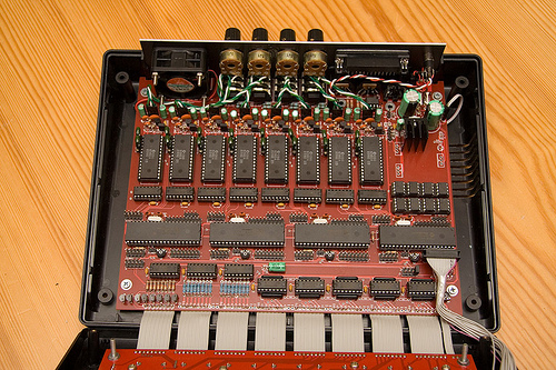
It's pure eye candy - not only outside, but also inside the case - TK's comment from MIDIbox of the Week
Well, there was my fifteen minutes… :)
I've received lots of praise for the design, but what I'm still amazed about is that so many people want one just like this. While designing it, I only catered for my needs, but still considered what might be useful for the few crazy SID fans who might want just the base PCB to upgrade their current MIDIbox SID to the new maximum of 8 SIDs. There are some people following this upgrade path, like TK and MTE, but with so many other people wanting one too, I decided it would be best if I did a few changes to suit everybody's needs.
The rest of this wiki page is thus relevant to people who bought or will buy the revised PCBs, whether just using the base PCB (with the PICs and SIDs on it) or the control surface PCB (with the switches, LEDs and rotary encoders).
PCB Specifications/Requirements
Base PCB
- The base PCB is essentially a merging of multiple MIDIbox modules into one compact PCB, and should work exactly the same as connecting multiple MIDIbox modules with cables. Almost all the ports on the Core module are available, with identical pinouts.
- The base PCB can be stuffed with (at most) 4x PIC18F4685, 8x SID, 8x 24LC512, 5x 74HC165 (40 digital inputs) 3x 74HC595 (24 digital outputs).
- The base PCB has 9v and 12v supply rails which you can connect to a pair of SIDs, so each pair of SIDs can be either 6581 SIDs or 8580/6582 SIDs.
- You don't have to use all the SID sockets. You can use from 1 to 8 SIDs. You can choose to put SIDs in stereo pairs, or only put a SID in the left SID socket for a mono channel.
- You don't have to use all the PIC sockets. You can choose to use less than four PICs.
- You don't have to use the DIN/DOUT at the bottom of the PCB, and you don't have to use the optimized switch/LED matrix I designed to get a “step C” control surface with only 8 shift registers, and you don't have to use a “step C” control surface (or any control surface). However, TK has kindly done all the code changes to support the optimized switch/LED matrix so you can have a big control surface with only the shift registers on this PCB.
- The base PCB is exactly 9200mil x 7215mil (9.2 inches x 7.215 inches). This fits exactly into the PT-10 case by PacTec, with mount holes that line up with the case standoffs.
- There are four different ways of supplying power to the base PCB:
- PSU Option A: C64 power supply, generating only 9v supply (no 12v) … exactly like the prototype, it converts the 9v AC coming from the C64 power supply. This option only allows use of SIDs that need 9v (8580 or 6582), the 6581 needs 12v. One 9v voltage regulator is used to supply 9v to all the SIDs.
- PSU Option B: C64 power supply, generating 9v and 12v supply … almost exactly like the "C64 PSU Optimized" circuit, which adds the 9v DC to the 5v DC to create 14v DC, enough to get the 12v required for 6581 SIDs. Instead of a voltage regulator on each SID module, there are just two (one 9v and one 12v).
- PSU Option C: Uses 5v regulation circuit to provide option A or B when not using C64 PSU (which has its own 5V regulation). I have added this option at the last minute to the PCB as a potential workaround for people unable to get a C64 PSU. People could generate 5v from a single unregulated 9v AC supply (9v AC adapter) or supply separate unregulated 9v AC and unregulated 5v DC supplies (9v and 5v AC adapters), using the same power socket and switch. Please do not assume this idea will work well, it might introduce noise, hum and heat!
- PSU Option D: External regulated power supply circuit, supplying +12v,+9v,+5v and ground … for those people wanting to use their own power supply, because they don't want to use the C64 PSU.
- PSU Option E: Uses a single 12-15V DC supply (aka a common wall-wart). This is a newer option worked out on the forums to avoid the common pitfalls associated with using a C64 power supply or other AC PSUs. Uses switching regulators (which were not available at a reasonable price or quality when the MB-6582 was designed) in order to generate a 5V rail (or a 5V and a 9V rail in the case of a mixed-SID setup) and a regular linear regulator to generate the 9v rail (or the 12V rail in the case of 6581/mixed-SID setups). Click the link for a complete tutorial.
Control Surface PCB
The control surface PCB is design to work with the parts described in the parts list:
MB-6582 Control Surface Parts List
These parts work with the 10mm gap between frontpanel and control surface PCB. Any variation in these parts (or the 10mm gap) will affect the end result.
PCB Revisions
Base PCB
The prototype base PCB was built for my needs, and my eight 6582 SIDs, so it only generates a 9 volt supply for the SIDs. I did consider generating both 9v and 12v (to support 6581 SIDs also), but there wasn't the space. Plus, this is the MB-6582, it will only ever have 6582 SIDs. So the biggest change to the base PCB is supporting all kinds of SIDs by optionally generating both 9v and 12v supplies. Since the base PCB was designed and the prototype made before TK finalized the hardware design, some changes were made when TK changed the hardware design. With the use of PIC18F4685, the IIC MIDI modules were redundant and removed, the CAN bus required and added, and all PICs were connected to the MIDI In port.
Control Surface PCB
The big change for the control surface PCB was dealing with the fact that people cannot buy the same 4×20 PLED display like in the original MB-6582, so the way I mounted the display between the PCB and panel cannot work with thicker LCD displays. Since it was possible for me to put the PLED display in the 10mm gap, the entire control surface was designed to accommodate this, which is why the original has two small PCBs above and below the display to hold the switches and LEDs.
In the revised design, there is a hole in the PCB and the LCD display is mounted behind the PCB, through this hole, and there is about a 2.5mm gap between the top of the LCD and the back of the frontpanel. The switches and LEDs above and below the display, which were mounted on separate PCBs in the original, are now mounted on the control surface PCB, so the same kind of switch can be used and construction will be a lot easier.
Building Your Own
There is a lot of documentation for people building their own. People must read everything before they start buying parts so they fully understand which parts are optional and which parts are required.
Follow the links to the other sections:
MB-6582 Base PCB Construction Guide
Panel Designs
Files for making or ordering your own panels can be found here:
Final PCB Designs
Revision 1 PCBs (bought from Wilba)
http://www.mb6582.org/plans/MB-6582_Base_PCB_Color.pdf dead link
http://www.midibox.org/dokuwiki/lib/exe/fetch.php?media=mb-6582:mb-6582_base_pcb.pdf
http://www.mb6582.org/plans/MB-6582_Base_PCB_Mono.pdf dead link
http://www.mb6582.org/plans/MB-6582_CS_PCB_Color.pdf dead link
http://www.mb6582.org/plans/MB-6582_CS_PCB_Mono.pdf dead link
Revision 2 PCBs (bought from SmashTV or Modular Addict)
http://www.mb6582.org/plans/MB-6582_Base_PCB_R2_Color.pdf dead link
http://www.midibox.org/dokuwiki/lib/exe/fetch.php?media=mb-6582:mb-6582_base_pcb_r2_color.pdf
http://www.mb6582.org/plans/MB-6582_Base_PCB_R2_Mono.pdf dead link
http://www.mb6582.org/plans/MB-6582_CS_PCB_R2_Color.pdf dead link
http://www.midibox.org/dokuwiki/lib/exe/fetch.php?media=mb-6582:mb-6582_cs_pcb_r2_color.pdf
http://www.mb6582.org/plans/MB-6582_CS_PCB_R2_Mono.pdf dead link
Control Surface Wiring
These describe the wiring of the control surface PCB. They can be used as a guide for constructing your own control surface. You can freely assign LEDs and switches to the matrix, but for the best performance in the firmware, the Modulation Matrix LEDs should be wired with common cathodes in vertical columns, so that the LED matrix will illuminate one column of 8 LEDs each shift register update.
LEDs and switches marked with an asterisk (*) are V2-specific features or just things I added for my own use. Refer to http://www.ucapps.de/midibox_sid_manual_fp.html for more information.
BTW I just noticed my CS DOUT wiring PDF is wrong… “LFO Sin” and “LFO Tri” are swapped and “Sync”, “CC”, “Edit”, “Play” are in the wrong order (should be “Play”, “Edit”, “CC”, “Sync”)
EDIT 2 - The menu button should be at the intersection of “JD8-D3 & JD5-D3” NOT “JD8-D3 & JD5-D4”
The rotary encoders are connected directly to the first four DIN modules on the base PCB (i.e. JD1 to JD4) as per the normal way of connecting rotary encoders to DIN modules. Just like the LEDs and switches, you can assign them to any pins of DIN modules and configure this in the table in the .asm file.
Questions and Answers About The MB-6582 Base PCB
Until I find a better place for this info, I'll put it here…
What is the function of J11 (directly below U1_Core1)?
J11 (not J11_CORE1) is a 4×2 pin header which controls which Core (PIC Tx pin) is connected to the MIDI Out port. You would only need to use this once for the first upload of MIOS and the MB-SID V2 firmware, thereafter connect the master PIC (1) to the MIDI out and after uploading new MB-SID V2 firmware, the master PIC can clone itself to the other PICs across the CAN bus. NOTE: All Cores (PIC Rx pin) are connected to the MIDI In port. The different device ID (0,1,2,3) on each PIC determines which PIC receives an upload, J11 is used to get “feedback” from that PIC during the upload.
What is the function of P1 (extreme lower right corner)?
LCD backlight brightness control, just like on the Core module.
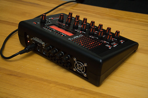
How are the attentuating pots pictured on the rear of the chassis connected?
These are not volume controls. These are for using feedback to get the SID to have distortion, or with Filter Ext In turned on, extra resonance when using band-pass, or LP+BP or HP+BP. They are dual-gang pots, connected to J3_SIDx and J23_SIDx. Input goes to wiper pin (middle pin). Ground goes to left pin (facing towards pot shaft, pins pointing down). Output goes to right pin (facing towards pot shaft, pins pointing down).
What sorts of heatsinks should be fitted for V3 and V1 (I am using Option B). Their positions seem to prevent both from having a sink at the same time. Should I look for flatter heatsinks?
Heatsinks may not be required, it all depends on how many SIDs you use and the load on the 9v and 12v supplies. But if you discover your regulators are getting hot, then you can add heatsinks.
I used these ones as a guide for placing the regulators far enough apart, giving enough space for both to be fitted. http://www.altronics.com.au/index.asp?area=item&id=H0640
Do not connect V1 and V2 to the same heatsink. Do not connect V1 and V3 to the same heatsink. Their common pins are different, V1's common pin is 9V above the common pins of V2 and V3.
If I'm using the PacTec PT-10 case, do the extra headers on the cores really need to be populated?
It all depends on whether you want to eventually connect analog inputs (pots, joysticks, etc.) or analog outputs (to control external filters) to the expansion port on the rear panel. Obviously some are truly unused and never likely to be used (like the IIC port and DIN/DOUT ports) but I put them all in there for full flexibility and compatibility with the Core module PCB. Basically, if you understand the Core module enough to know they aren't needed, then it's up to you whether to populate them.
I choose to fully populate the PCB so that I don't ever need to solder it again, and it looks better than empty holes on the PCB. I suggest people do the same, for the advantages should you need to troubleshoot, but ultimately you're free to do what you like.
At a minimum I recommend at least populating the J15 headers (for LCD) so you can troubleshoot slave cores easily by connecting an LCD (should things stop working!)
Likewise, do I really need to mount pot P2 for the slave cores?
As above, these are the contrast pots for LCDs so they're only useful for troubleshooting. If you want to save on trim pots, you could short between the middle pin and the left or right pin, this would approximate turning the trimpot fully one way and at least let the LCD display something when connected to slave PICs.
The tiny jumper pads on the solder side beneath the cores have something to do with 8-bit mode for LCDs. How are these supposed to be set?
Connect ribbon cable to the LCD or PLED using all wires, as if you were going to use 8-bit mode on a normal Core module. The four wires you don't need for 4-bit mode are not connected on J15 by default. If you discover your display freezing up after a while (but the synth still works in the background), you can execute a MIOS memory read from MIOS Studio to validate that the display has timed out, most likely due to a bug working in 4-bit mode. To fix this, you can run in 8-bit mode by using two PIC pins from port E to replace the two PIC pins being used by the CAN bus. Solder those jumper pads on the bottom side, run the change device ID app to use custom LCD driver, the custom LCD driver file should already be in the source code of the MB-SID V2 application and compiled in. If you want to run other applications, you'll need to copy that custom LCD driver file into those source directories and rebuild those applications.
Is there any reason why 16-volt 2200uF caps cannot be used instead of 25-volt ones?
For the 5v supply: no. For the 9v AC after the bridge rectifier: not really. I was told once to expect up to 2x the voltage after the rectivier, i.e. if it's 9v AC, choose capacitor to handle 18v DC. It really doesn't go up that high I think, and caps rated to 15v should be enough.
The silkscreen for the diode in each core has a via right in the middle, obscuring the arrow. Which direction is the arrow pointing?
The diode is pointing down. Cathode on the lower pin. Refer to the PCB PDFs for more detail.
What's the purpose of the J70 header?
This is a passive mixed output of the four stereo channels, which you can connect to the small phono jack above the power switch. Totally optional.
This was a late design idea I threw into the prototype, the resistors below each audio socket are used to connect the audio signals together when there is no plug in the switched audio socket, i.e. it will only mix those sockets without plugs. You need to connect it together with insulated wire under the board though…. I didn't want to mess up the ground plane with tracks. To the right of the resistors R70-R77 (below the stereo sockets) are pads, these pads should be connected in two sets of wires, one set connects the pads that are next to R70, R72, R74, R76, the other set connects the pads that are next to R71, R73, R75, R77. (NOTE: R2 boards do not require the wires, there are tracks on the top layer.)
I used 10K resistors there because that's what I've seen before in passive mixer designs, but the output is very attenuated, and I am guessing that you could drop these to 1K or less, as the outputs of the audio buffers after each SID can probably handle that. Someone with more audio electronics (and SID!) knowledge can probably answer that question.
I am troubleshooting my LED's and need that cool utility that makes everything light up
It can be found here: http://midibox.org/forums/index.php?/topic/9669-mb-6582-led-matrix-issue/page__view__findpost__p__77144

