Table of Contents
AIN_4 module
This is a simple way of scaling CVs (as might come from a modular) ready for an STM32F4 Core module.
Schematic
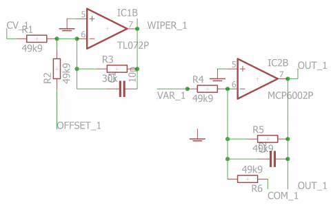
The circuit is a very simple series of two inverting amplifiers per channel. The first is a TL072 powered from +12/-12V, while the second is an MCP6002 powered from 3v3/0V (ground). It's possible to preset the ranges (see below) but it's probably more useful to use the associated Control Board.
For bipolar operation, a +5V reference may be switched in. The output of the first stage is interrupted by a pot in order to attenuate the signal. The second stage has switchable gain from -1 to -0.5 by way of a resistor. Hence one can easily select between 0-5V, 0-10V and +/- 5V input ranges to optimise the signal amplitude reaching the ADC. Because the second op amp is powered at the same voltage as the MCU (ideally the same rail), its inputs are protected from over- and under-voltages.
Note the gain calculation, and beware the top of the signal may clip (harmlessly) if around 3.0V peak is exceeded on the second op amp stage.
BOM v1.2
| Type | Qty | Value | Package | Parts | Notes |
|---|---|---|---|---|---|
| resistors | |||||
| 20 | 49k9 1% or better | 0204/7 | R1, R2, R4, R5, R6, R7, R8, R10, R11, R12, R13, R14, R16, R17, R18, R19, R20, R22, R23, R24 | 49k9/30k resistors aren't so common. For almost equivalent behaviour, one could substitute e.g. 56k/33k. It's best to match pairs/threes or go for 0.1% tolerance parts | |
| 4 | 30k 1% | 0204/7 | R3, R9, R15, R21 | nominal gain can be adjusted e.g. (22k/49.9k)*5V = 2.2V | |
| capacitors | |||||
| 4 | 10p | 025×050 | C1, C3, C5, C7 | ||
| 9 | 100n | 025×050 | C10, C12, C13, C14, C15, C16, C17, C18, C20 | remove 1 if powering from Core | |
| 3 | 10u | electrolytic 2,5-6 | C9, C11, C19 | remove 1 if powering from Core | |
| 4 | optional | 025×050 | C2, C4, C6, C8 | can use another e.g. 10pF cap here for more filtering | |
| inductors | |||||
| 2 | BEAD | 5MM | L1, L2 | or replace with wire link | |
| ICs | |||||
| 2 | MCP6002P | DIL08 | IC2, IC4 | sockets are recommended | |
| 2 | TL072P | DIL08 | IC1, IC3 | sockets are recommended | |
| Vreg | |||||
| 1 | optional | TO-220 | VR1 | remove if powering from Core | |
| headers | |||||
| 7 | 1X02_SMALL | JP1, JP2, JP3, JP4, JP5, JP6, JP7 | check board for headers as SIL strips of 3, 5 or 6 | ||
| 8 | 1X03_SMALL | JP8, JP9, JP10, JP11, JP12, JP13, JP14, JP15 | |||
| 2 | 2*5 (shrouded) | J1, J2 |
Versions
v1.2: first release.
Assembly
Putting the board together is simple. As usual, start with the flattest components and work your way up.
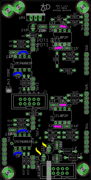
Resistors
- four 30k resistors marked in pink
- remainder are 49k9
- for best results, match R1/R2, R7/R8 (and so on), and R4/R5/R6, R10/R11/R12 (and so on).
- the value is less important than the minimum deviation.
Capacitors
- four 10p as marked in pink
- electrolytics in yellow
- blue are optional (i.e. probably unnecessary)
- remainder are 100n.
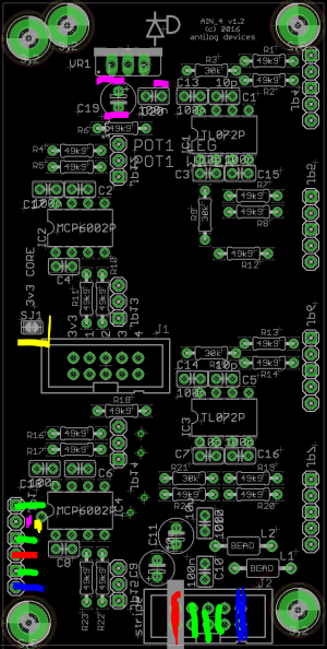
Power
- J2 is a standard Eurorack header
- red = -12V
- blue = +12V
- green = 0V(ground)
- for Core power, bridge the solder jumper marked in yellow
- otherwise install the Vreg circuit in pink
- IMPORTANT only choose one of these 3v3 power options! Don't install the regulator if the solder jumper is bridged.
Headers
For connection to a Control Board, use pin headers placed on the opposite side as the rest of the components i.e. follow the silkscreen markings. It's convenient to use an unsoldered Control Board to align all of the pins at once.
For standalone use, you probably want header pins (or sockets, or even bare wires if you wish) on the same side as the remaining circuitry.
Standalone use
For simplest results, use the complementary Control Board. Otherwise see below for header functions (viewed from the component side).
Five pin header
- IN = CV input
- for scaling bipolar CVs, connect or switch into OFFSET (e.g. +5V; n.b. the offset should be referenced to the common 0V)
- for 0-5V operation, leave SWITCH open; for 0-10V operation, jumper or switch in COMMON to POLE
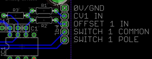
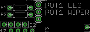
Three pin header
- with a 100k pot facing you, solder the left leg to 0V(ground)
- with the pot turned anticlockwise, the TL072 output is shorted to ground. While shorts are permitted in the datasheet, it's advisable to connect a small value resistor (e.g. 10-100R) between the left leg and ground.
- centre to WIPER
- right to LEG
- WIPER and LEG may be jumpered if pots aren't desired, but it is quite useful to have an attenuator to trim down variable CVs or even clip the second op amp for crunchy waveforms!
Interconnection to Core
J1 carries the scaled CV to J5A or J5B of an STM32F4 Core module.
License
Currently the design is © 2016 antilog devices with all rights reserved; all documentation is CC BY-NC-SA 3.0.