Table of Contents
OLRE16


Introduction
The Start point was a search about a good LED-Ring for encoders Forum thread .
2 existing solutions , but that could be improved :
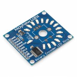
- The LED Ring Breakout Board from Sparkfun Big, single blue color and only 16 segments.
- Fairlightii LRE8x2CS..Monochrome, Only 16 segments
Improvement Guidelines
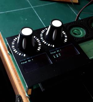
- RGB LEDs for enhanced user feedback and further possible interactions
- 31 segments in a 270° open ring + 1 index/step segment.
- A straight aligned 16 rings board would fit in a 19“ rack
- Small screen to display values like step#, name of the parameter
- PCB-mount under front panel has to be easy and should stack the other board which supports the encoders.
- Interface with to mios32 core has to be easy.
The Result
LED Driving
Sizing
We expect 16 RGB LED rings encoders. So let's do the math :
16 Encoders * 32 LEDs * 3 colors = 1536 lines
Let's transpose this to a classical matrixed SRIO chain design:
16 * 3 (cathodes) * 32 (anodes)
= 48 inputs + 32 outputs
= 6*DIN + 4*DOUT
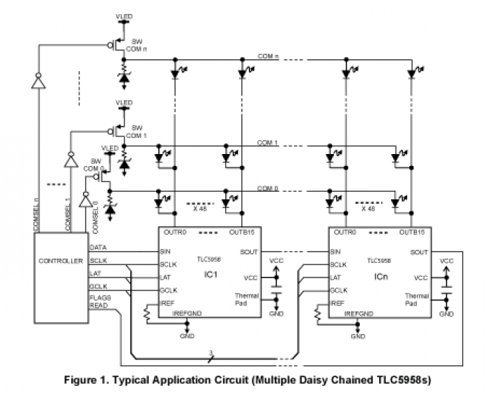
Core-External Driving Concept : TLC5958
In theory it's possible to drive such a SRIO setup but in fact buses and resistors/R networks are very hard to place and it will consume a lot of contant refresh process.
After a look on the different brands and models of LED driver IC Texas Instruments TLC5958 appeared as a good compromise to drive a lot of RGB LEDs without overloading the core. Designed to be a LED Display driver, its original purpose and features would allow large-sized RGB-LED-based display setups
TLC5958 Datasheet
This Design note from Texas Instruments helps in understanding how to design around the TLC:
Build high density, high refresh rate, multiplexing LED panel with TLC5958
TLC5958 Features
- 48 Channels Constant Current Sink Output
- Global Brightness Control (BC) : 3-Bit (8 Step)
- Color Brightness Control (CC) for Each Color Group: 9-Bit (512 Step), Three Groups.
- Grayscale(GS) Control with Multiplexed Enhanced Spectrum(ES) PWM: 16bit
- 48K bit Grayscale Data Memory Support
- 32-multiplexing ( 32 lines mux * 48 channels = 1536!)
- SPI Data Transfer Rate: 25MHz
- LED Open Detection (LOD)
- Thermal Shut Down (TSD)
- IREF Resistor Short Protection (ISP)
- Delay Switching to Prevent Inrush Current
- Pre-charge FET to Avoid Ghosting Phenomenon
- Daisy-Chain!
Mechanical Design
Initial goal was to fit 16 LED Rings + bottom OLEDs in a 19” rack.
19“ = 440mm.
440 - (4mm case side)*2 = 432 mm.
432/16 LED-Rings = 27mm / LED-Ring
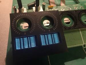
Luckily an OLED 0.96” is exactly sized 27mm
The total height is 50mm, with the mounting holes.
1 Rack Unit size height (44.5mm) was impossible with the OLED displays. Note that it's possible without.
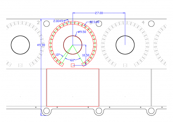
By reversing OLED displays, the active area is closer to the ring.
Distance between SMD LEDs center is somewhat close (2.0046mm) But not impossible, for proof:
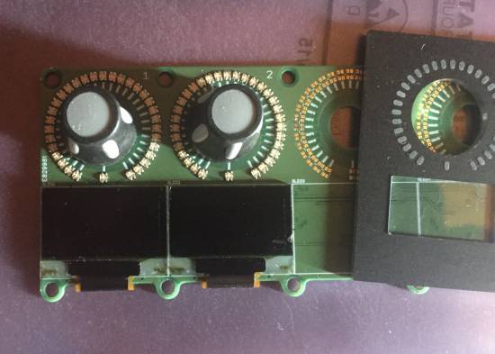
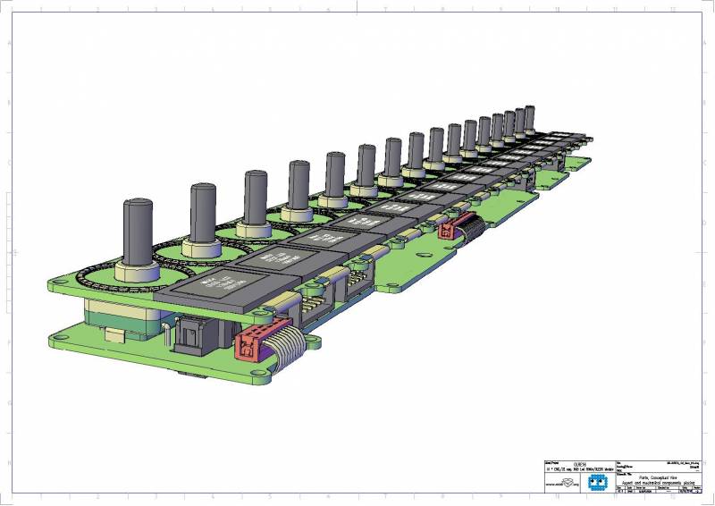
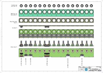
Conceptual views
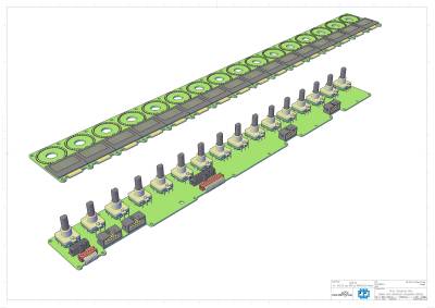
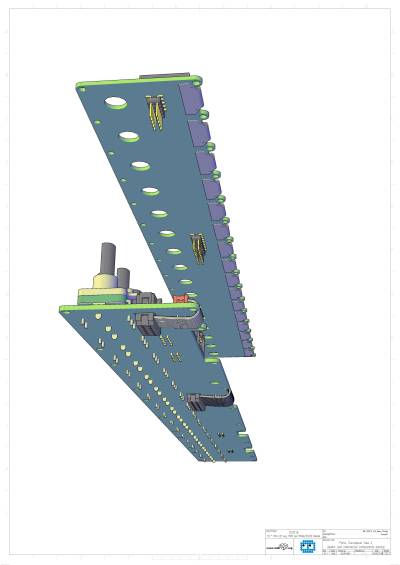
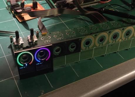
The module consists in a 2 pcbs sandwich, spaced 10mm .
Global size is 432mm Width * 50mm Height * 22mm Depth
Prototyping
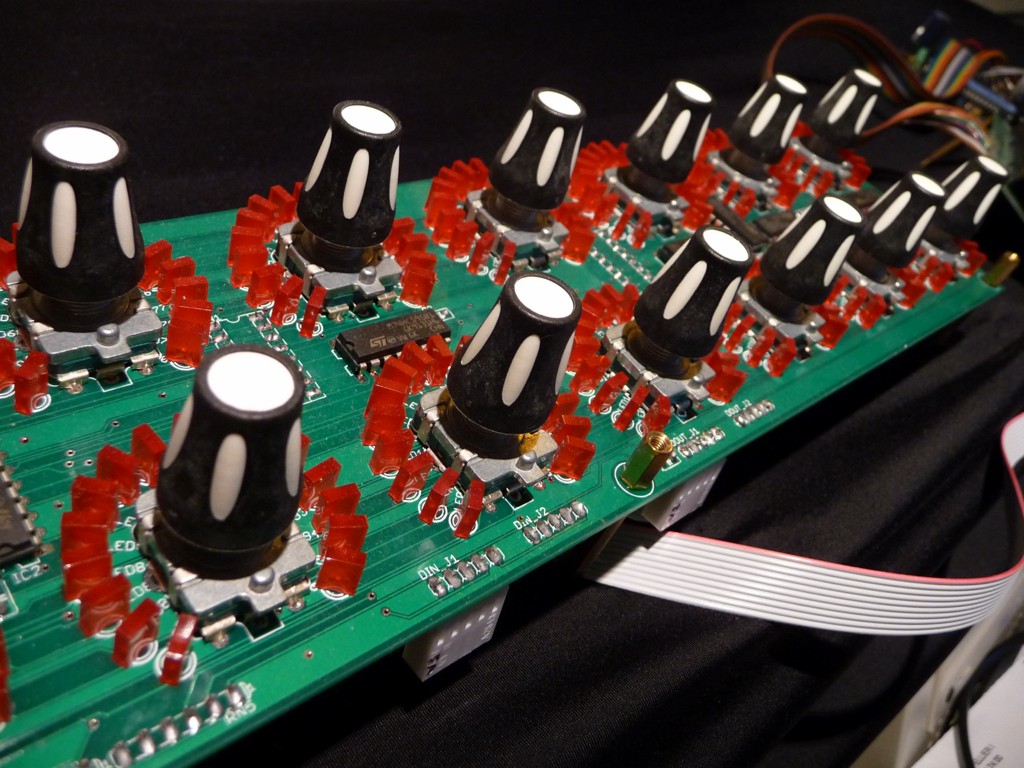
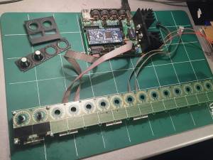
The first prototype was tested with an LPC1769 Core. For testing purposes only 2 LED-rings were set up in order not to waste components for development.The first software module written was added in an app, but integration in the SEQ V4 app was not possible because a lack of Memory on the LPC17 Core…
Meanwhile the migration to STM32F4 Core, an independent external clocking circuit for the GSCLK and the address lines was designed. STM32F4 Core will just have to provide a PWM a RESET signal and receive an interrupt from this circuit to get the End Of Frame.
Data Transfer
A serialized design has been chosen to provide data to TLC. Prototype feature only 2 steps but the CORE works like there's 4 modules of 16 steps connected. In order to benchmark reactivity and Transfer time, Core send data for 4 modules(4*16*32*3*16bit=12KBytes). Through an emulated software SPI bus, for this 64 rings Data Sending takes less than 5ms . Different colors and patterns like relative value(-64/63), keyboard(B&W keys) etc… were tested.
GrayScale Clock
Design of External GrayScale Clock for the TLC was tricky.
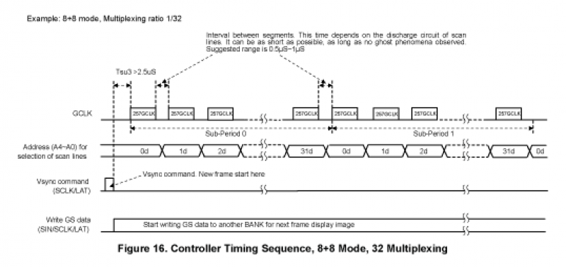
257 clock periods and halt for some 1.5~2.5µs are needed for each address line
TLC would receive a VSYNC command at the end of the 32th address line to prepare the new frame datas.
The first approach was to provide a PWM at 800KHz and put it back to the LPC on a TMR CAP Input, use 2 MAT outputs to provide a line period and gate(NOR) the PWM with it.
First issue, halting time after the 257 periods wasn't constant and dependent of PWM frequency. Second issue, much I/O used only for this purpose.
Electronic Design
TLC related Design
TLC is wired like on an SPI bus to Core Board. Here are connections equivalences:
- SCLK ⇒ SC
- DATA ⇒ SO
- LAT ⇒ RC
- FLAGS READ ⇒ SI
STM32F4 I/O Ports
Note: Command is coded by putting LAT active during a defined number of SCLK periods.For example for a VSYNC command, LAT must be high during 3 SCLK pulses.
TLC5958 don't need to have data sent for each multiplex address like for the BLM.
Frame update is needed only when a change occurs, TLC keep all the frame in memory and continue to distribute it to the 32 addresses lines and 16 rgb leds by address
GrayScale Clock
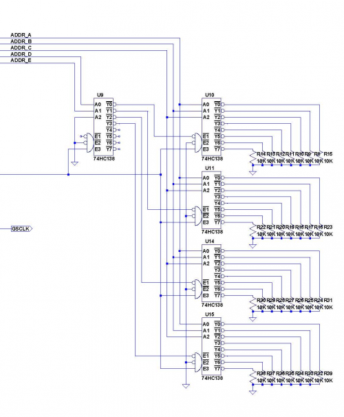
The TLC needs a GrayScale Clock(GSCLK) and additional control to multiplex 32 addresses (named COMSELx in diagram). The GSCLK signal should be 257 pulses + 1.5~2.5µs of interval between segments . COMSEL management needs 32 multiplexing adress lines for (5 bits coded and decoded directly on the top board).
Clock Schematic version 1
Note: This circuit is replaced by a simulated one, on a CPLD.
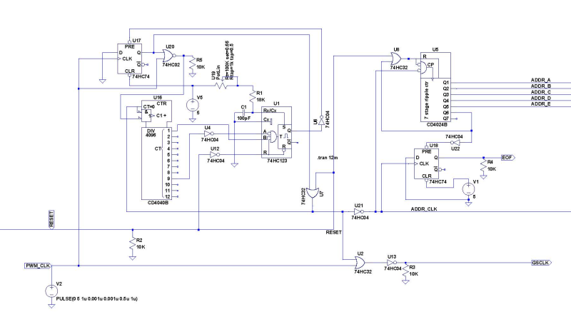
The external clock circuit was simulated on LTSpice first and tested on veroboard with the prototyped OLRE16.
PWM_CLK, RESET and EOF are connected to the CORE
CORE provides a regular Clock with PWM @2MHz .The 12bit counter U16 counts until 257 and trigs U1 wich is a monostable, U1 switchs, resets the counter and stops the clock counter input by U17(D-Flipflop).
After a certain time given by the RC couple on U1, U1 switchs back and restarts the counter.
By this way we are sure to count the exact 257 Clocks needed and the interval between 2 segments is fixed by the trimpot U19.
GSCLK signal is then high during the 257 clocks period and low during the interval
Multiplexing Schematic
ADDR_x, ADDR_CLK, GSCLK are connected to the top board…
ADDR_CLK is the multiplexed lines clock . It's used to gate the PWM signal and obtain the GSCLK and of course, as a clock for the ADDR Counter U5. The counter U5 provides the coded ADDR_x lines and an EOF(End Of Frame) when 32 is reached.
Clock version 2
CPLD/FPGA version
To be continued… 

